Section 17 I
2
C Bus Interface 3
Page 880 of 2108 R01UH0134EJ0400 Rev. 4.00
Sep 24, 2014
SH7262 Group, SH7264 Group
12 781 7812
SCL
MST
TRS
RDRF
ICDRS
ICDRR
SDA
(Input)
Bit 0
Bit 6 Bit 7 Bit 0 Bit 6 Bit 7 Bit 0 Bit 1
Bit 1
User
processing
Data 1
Data 1
Data 2
Data 2
Data 3
[2] Set MST
(when outputting the clock)
[3] Read ICDRR [3] Read ICDRR
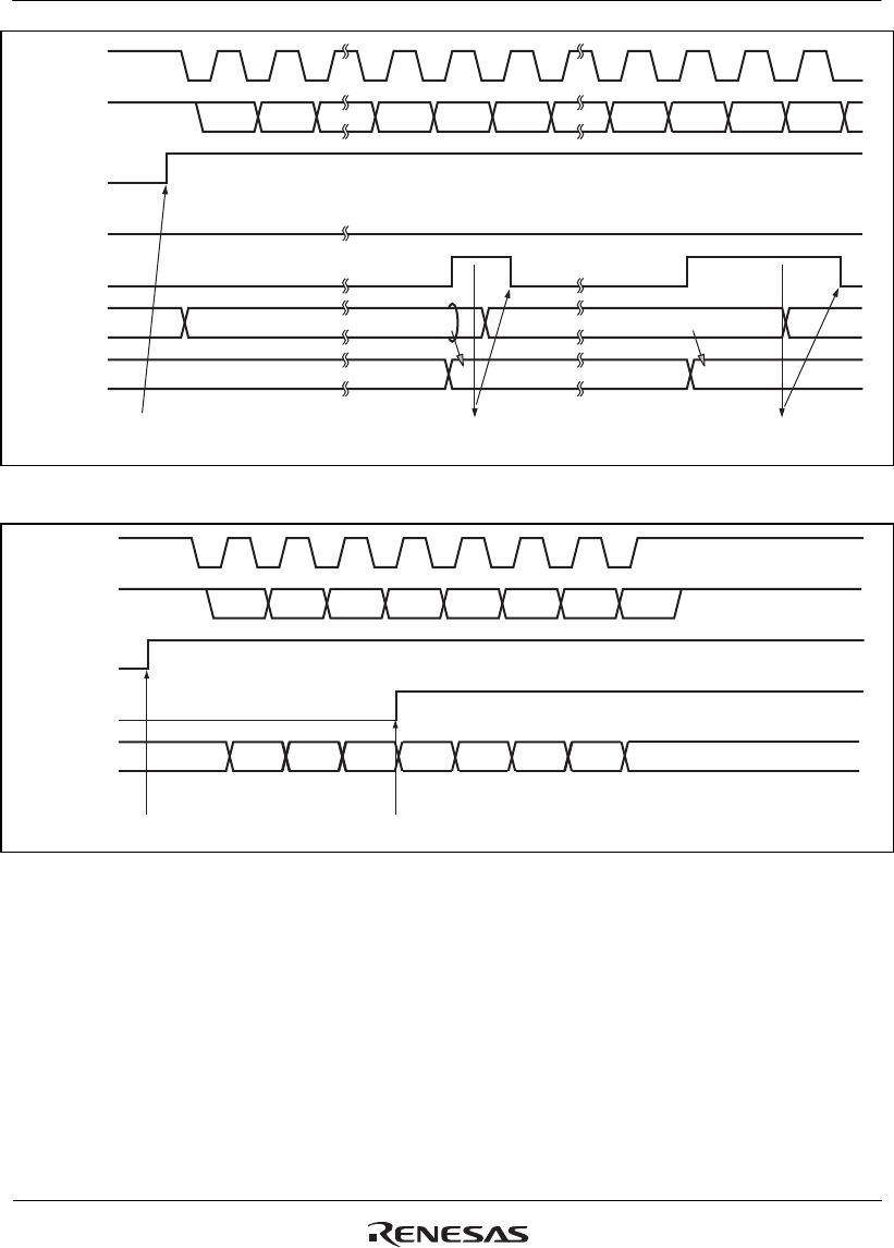
Figure 17.15 Receive Mode Operation Timing
12345678
000
SCL
MST
RCVD
111 110 101 100 011 010 001 000
SDA
(Input)
Bit 0 Bit 1 Bit 2 Bit 3 Bit 4 Bit 5 Bit 6 Bit 7
BC2 to BC0
[2] Set MST
[3] Set the RCVD bit after checking if BC2 = 1
Figure 17.16 Operation Timing For Receiving One Byte (MST = 1)


