R01UH0134EJ0400 Rev. 4.00 Page 2093 of 2108
Sep 24, 2014
Item Page Revision (See Manual for Details)
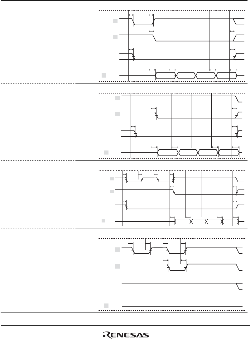
37.4.3 Bus Timing
Figure 37.28 Synchronous
DRAM Burst Write Bus Cycle
(Four Write Cycles) (Bank
Active Mode: ACT + WRITE
Commands, WTRCD = 0
Cycle, TRWL = 0 Cycle)
2003 Figure amended
D15 to D0
t
RASD1
t
RASD1
RAS
t
CASD1
t
CASD1
CAS
t
DQMD1
t
DQMD1
DQMxx
t
WDH2
t
WDD2
t
WDH2
t
WDD2
Figure 37.29 Synchronous
DRAM Burst Write Bus Cycle
(Four Write Cycles) (Bank
Active Mode: WRITE
Command, Same Row
Address, WTRCD = 0 Cycle,
TRWL = 0 Cycle)
2004 Figure amended
D15 to D0
RAS
t
CASD1
t
CASD1
CAS
t
DQMD1
t
DQMD1
DQMxx
t
WDH2
t
WDD2
t
WDH2
t
WDD2
Figure 37.30 Synchronous
DRAM Burst Write Bus Cycle
(Four Write Cycles) (Bank
Active Mode: PRE + ACT +
WRITE Commands, Different
Row Addresses, WTRCD = 0
Cycle, TRWL = 0 Cycle)
2005 Figure amended
t
RASD1
t
RASD1
t
RASD1
t
RASD1
D15 to D0
RAS
t
CASD1
t
CASD1
CAS
t
DQMD1
t
DQMD1
DQMxx
t
WDH2
t
WDD2
t
WDH2
t
WDD2
Figure 37.31 Synchronous
DRAM Auto-Refreshing
Timing (WTRP = 1 Cycle,
WTRC = 3 Cycles)
2006 Figure amended
t
RASD1
t
RASD1
t
RASD1
t
RASD1
D15 to D0
RAS
t
CASD1
t
CASD1
CAS
(Hi-Z)
DQMxx


