Section 9 Bus State Controller
R01UH0134EJ0400 Rev. 4.00 Page 323 of 2108
Sep 24, 2014
SH7262 Group, SH7264 Group
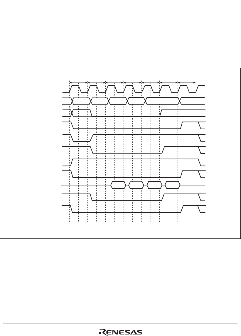
When bank active mode is set, if only access cycles to the respective banks in the area 3 space are
considered, as long as access cycles to the same row address continue, the operation starts with the
cycle in figure 9.20 or 9.23, followed by repetition of the cycle in figure 9.21 or 9.24. An access to
a different area during this time has no effect. If there is an access to a different row address in the
bank active state, the bus cycle in figure 9.22 or 9.25 is executed instead of that in figure 9.21 or
9.24. In bank active mode, too, all banks become inactive after a refresh cycle or after the bus is
released as the result of bus arbitration.
Tc4Tr Tc2 Tc3Tc1
Td4Td2 Td3
Td1
Tde
CKIO
A25 to A0
CS3
RD/WR
RAS
DQMx
D15 to D0
BS
DACKn*
2
A12/A11*
1
CAS
Notes: 1. Address pin to be connected to pin A10 of SDRAM.
2. The waveform for DACKn is when active low is specified.
Figure 9.20 Burst Read Timing (Bank Active, Different Bank, CAS Latency 1)


