Section 9 Bus State Controller
R01UH0134EJ0400 Rev. 4.00 Page 305 of 2108
Sep 24, 2014
SH7262 Group, SH7264 Group
T1
CKIO
A25 to A0
CS5
RD/WR
RD
D15/D7 to D0
WEn
D15/D7 to D0
BS
Read
Write
T2
DACKn*
Ta1 Ta2 Ta3
AH
Address
Address Data
Data
Tadw Tw Twx
WAIT
Note: * The waveform for DACKn is when active low is specified.
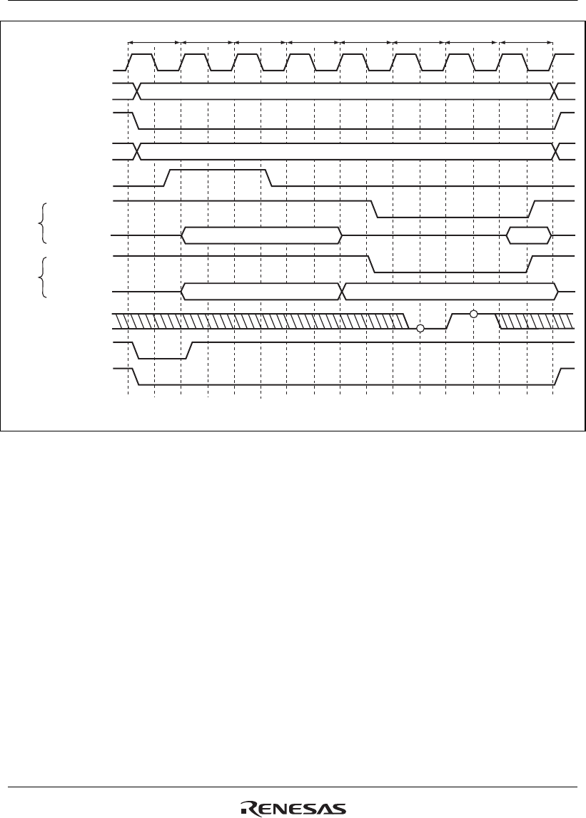
Figure 9.13 Access Timing for MPX Space
(Address Cycle Access Wait 1, Data Cycle Wait 1, External Wait 1)


