Section 27 Video Display Controller 3
R01UH0134EJ0400 Rev. 4.00 Page 1601 of 2108
Sep 24, 2014
SH7262 Group, SH7264 Group
27.7.21 Graphics Image Line Offset Registers (GROPSOFST1 and GROPSOFST2)
31 30 29 28 27 26 25 24 23 22 21 20 19 18 17 16
15 14 13 12 11 10 9 8 7 6 5 4 3 2 1
0
0000000000000000
R R R R/W R/W R/W R/W R/W R/W R/W R/W R/W R/W R/W R/W R/W
0000000000000000
R/W R/W R/W R/W R/W R/W R/W R/W R/W R/W R/W R/W R/W R/W R/W R/W
- - - GROPSOFST[28:16]
GROPSOFST[15:0]
Bit:
Initial value:
R/W:
Bit:
Initial value:
R/W:
Bit Bit Name Initial Value R/W Description
31 to 29 All 0 R Reserved
These bits are always read as 0. The write value
should always be 0.
28 to 0 GROPSOFST
[28:0]
H'00000000 R/W These bits specify the line offset for the graphics
image.
In 16-byte burst transfer: The lower four bits should
always be 0000.
In 128-byte burst transfer: The lower seven bits
should always be 000_0000.
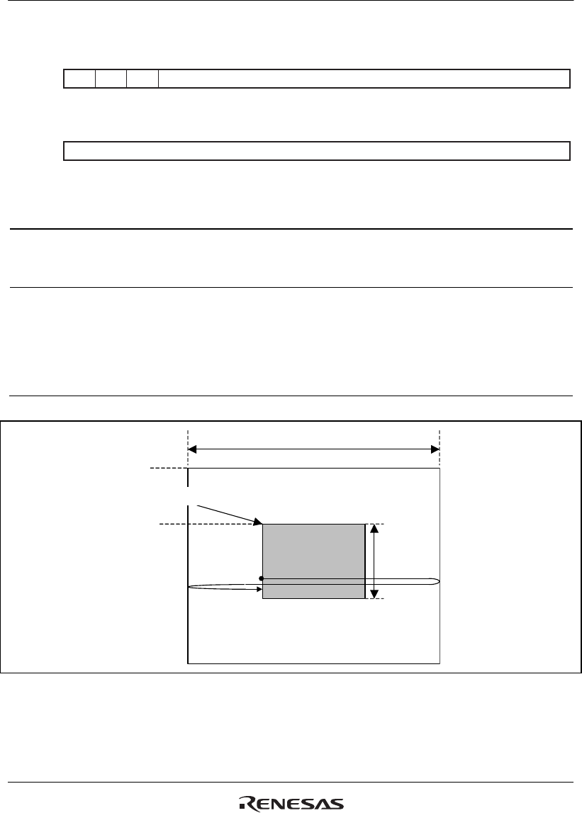
Display memory area
GROPSADR1, 2
GROPSOFST1, 2
Graphics image
area
Figure 27.21 Graphics Image Memory Area Settings
The start (left side) address of line n is obtained by adding the base address register value
(GROPSADR1 or GROPSADR2) and the line offset (GROPSOFST1 or GROPSOFST2) n.


