Section 9 Bus State Controller
R01UH0134EJ0400 Rev. 4.00 Page 317 of 2108
Sep 24, 2014
SH7262 Group, SH7264 Group
Tc4 (Tap)Tr Tc2 Tc3Tc1
Td4
Tde
Td2 Td3
Td1
Trw
Tw
CKIO
A25 to A0
CSn
RD/WR
RAS
DQMx
D15 to D0
BS
DACKn*
2
A12/A11*
1
CAS
Notes: 1. Address pin to be connected to pin A10 of SDRAM.
2. The waveform for DACKn is when active low is specified.
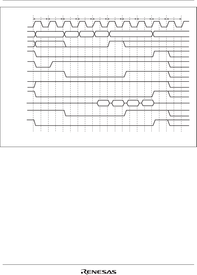
Figure 9.16 Burst Read Wait Specification Timing
(CAS Latency 2, WTRCD[1:0] = 1 Cycle, Auto Pre-Charge)


