Section 35 Motor Control PWM Timer
R01UH0134EJ0400 Rev. 4.00 Page 1839 of 2108
Sep 24, 2014
SH7262 Group, SH7264 Group
35.3.6 PWM Buffer Registers_nA, nC, nE, nG (PWBFR_nA, PWBFR_nC, PWBFR_nE,
PWBFR_nG) (n = 1, 2)
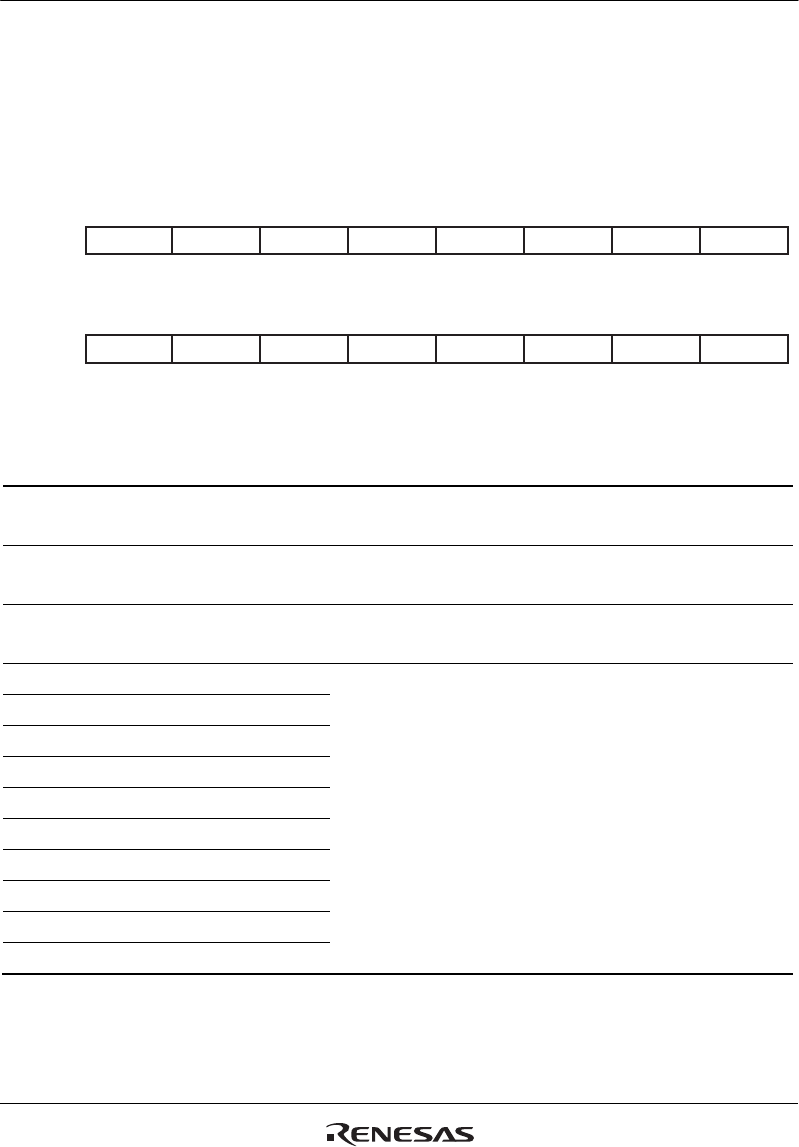
There are four PWBFR_n registers (PWBFR_nA, PWBFR_nC, PWBFR_nE, and PWBFR_nG).
When a PWCYR_n compare match occurs, data is transferred from the buffer register
(PWBFR_n) to the duty register (PWDTR_n).
15
—
1
R
14
—
1
R
13
—
1
R
12
OTS
0
R/W
11
—
1
R
8
DT8
0
R/W
10
—
1
R
9
DT9
0
R/W
Bit:
Initial Value:
R/W:
7
DT7
0
R/W
6
DT6
0
R/W
5
DT5
0
R/W
4
DT4
0
R/W
3
DT3
0
R/W
0
DT0
0
R/W
2
DT2
0
R/W
1
DT1
0
R/W
Bit:
Initial Value:
R/W:
Bit Bit Name
Initial
Value R/W Description
15 to 13 All 1 R Reserved
These bits are always read as 1 and cannot be modified.
12 OTS 0 R/W Output Terminal Select
Holds the data to be sent to bit 12 in PWDTR_n.
11, 10 All 1 R Reserved
These bits are always read as 1 and cannot be modified.
9 DT9 0 R/W Duty
These bits hold the data to be sent to bits 9 to 0 in
PWDTR_n.
8 DT8 0 R/W
7 DT7 0 R/W
6 DT6 0 R/W
5 DT5 0 R/W
4 DT4 0 R/W
3 DT3 0 R/W
2 DT2 0 R/W
1 DT1 0 R/W
0 DT0 0 R/W


