


Section 16 Renesas Serial Peripheral Interface
R01UH0134EJ0400 Rev. 4.00 Page 821 of 2108
Sep 24, 2014
SH7262 Group, SH7264 Group
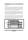
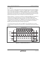
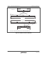
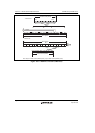
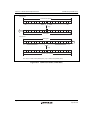
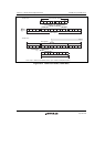
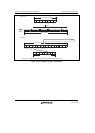
(4) LSB First Transfer (32-Bit Data)
Figure 16.11 shows the operation of the transmit buffer (SPTX) and the shift register when this
module performs a 32-bit data length LSB-first data transfer.
The CPU or direct memory access controller writes T31 to T00 to the transmit buffer. If the shift
register is empty, this module reverses the order of the bits of the data in the transmit buffer,
copies it to the shift register, and fully populates the shift register. When serial transfer starts, this
module outputs data from the MSB (bit 31) of the shift register, and shifts in the data from the
LSB (bit 0) of the shift register. When the RSPCK cycle required for the serial transfer of 32 bits
has passed, data R00 to R31 is stored in the shift register. In this state, this module copies the data,
in which the order of the bits is reversed, from the shift register to the receive buffer, and empties
the shift register.
If the receive buffer does not have a space for the receive data length after receive data has been
copied from the shift register to the receive buffer, another serial transfer will not be started. In
order to start another serial transfer, data for the receive data length should be read from the
receive buffer to secure the necessary space in the receive buffer.
If another serial transfer is started before the CPU or direct memory access controller writes to the
transmit buffer of the SPDR, received data R00 to R31 is shifted out from the shift register.