


Section 37 Electrical Characteristics
R01UH0134EJ0400 Rev. 4.00 Page 1963 of 2108
Sep 24, 2014
SH7262 Group, SH7264 Group
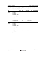
37.3 DC Characteristics
Conditions used to obtain DC characteristics (2) in table 37.2 other than current consumption
(for both 1-Mbyte and 640-Kbyte versions)
V
CC = PLLVCC = USBDVCC = USBUVCC = 1.1 to 1.3 V,
PV
CC = USBDPVCC = 3.0 to 3.6 V, AVCC = 3.0 to 3.6 V, USBAVCC = 1.1 to 1.3 V,
USBAPV
CC = 3.0 to 3.6 V, VSS = PLLVSS = AVSS = USBDVSS = USBAVSS = USBDPVSS =
USBAPV
SS = USBUVSS = 0 V, Ta = 20 to 85 C (regular specifications), 40 to 85 C (wide-
range specifications)
Conditions used to obtain DC characteristics (2) in table 37.2 for current consumption (1-
Mbyte and 640-Kbyte versions)
V
CC = PLLVCC = USBDVCC = USBUVCC = 1.2 V, PVCC = USBDPVCC = 3.3 V, AVCC = 3.3 V,
USBAV
CC = 1.2 V, USBAPVCC = 3.3 V, VSS = PLLVSS = AVSS = USBDVSS = USBAVSS =
USBDPV
SS = USBAPVSS = USBUVSS = 0 V, Avref = 3.3 V, VBUS = 5.0 V
T
a = 20 to 85 C (regular specifications),
40 to 85 C (wide-range specifications)
I = 144.00 MHz, B = 72.00 MHz, P = 36.00 MHz
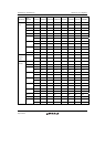
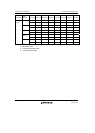
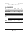
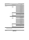
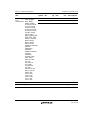
Table 37.2 DC Characteristics (1) [Common Items]
Item Symbol Min. Typ. Max. Unit Test Conditions
Power supply voltage PV
CC 3.0 3.3 3.6 V
VCC 1.1 1.2 1.3 V
PLL power supply voltage PLLVCC 1.1 1.2 1.3 V
Analog power supply voltage AVCC 3.0 3.3 3.6 V
USB power supply voltage USBAPVCC
USBDPVCC
3.0 3.3 3.6 V
USBAVCC
USBDV
CC
USBUV
CC
1.1 1.2 1.3 V
Input leakage
current
All input pins |Iin| 1.0 A Vin =
0.5 to PV
CC
– 0.5 V
Three-state
leakage current
All input/output
pins, all output
pins (except PE5
to PE0)
(off state)
|I
STI| 1.0 A Vin =
0.5 to PV
CC
– 0.5 V
PE5 to PE0 10 A
Input capacitance All pins Cin 20 pF