


Page 2078 of 2108 R01UH0134EJ0400 Rev. 4.00
Sep 24, 2014
Item Page Revision (See Manual for Details)
18.5.1 Limitations from
Underflow or Overflow during
DMA Operation
937 Description amended
... After this, for receive operation write 0 to the error status
flag bit to clear the error status, make settings to the direct
memory access controller again, and restart the transfer.
For transmit operation perform a software reset, then start
again from the start sequence.
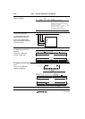
20.2 Architecture
Figure 20.1 This Module
Architecture
983 Figure note added
Note: Longword (32-bit) accesses are converted into two
consecutive word accesses by the bus interface.
Timer
985 Description amended
Contains registers such as TCNTR, TTCR0, CMAX_TEW,
RFTROFF, TSR, CCR, CYCTR, RFMK, TCMR0, TCMR1,
TCMR2 and TTTSEL.
20.3.3 Control Registers
(2) General Status Register
(GSR)
GSR (Address = H'002)
1011 Table amended
Bit 1: GSR1 Description
0 [Reset condition] When (TEC < 96 and REC < 96) or Bus Off (Initial value)
1 [Setting condition] When 96 ≤ TEC < 256 or 96 ≤ REC < 256
Bit 0: GSR0 Description
0 [Reset condition]
Recovery from bus off state or after a HW or SW reset (Initial value)
1 [Setting condition] When TEC ≥ 256 (bus off state)
...
20.3.5 Timer Registers
(1) Time Trigger Control
Register0 (TTCR0)
1040 Description and table amended
Bit 14 — TimeStamp value: Specifies if the Timestamp for
transmission and reception in Mailboxes 15 to 0 must ...
Bit14: TTCR0 14 Description
0 CYCTR[15:0] is used for the TimeStamp in Mailboxes 15 to 0 (initial v alue)
1 CCR[5:0] + CYCTR[15:6] is used for the TimeStamp in Mailboxes 15 to 0
21.3.16 IEBus Transmit
Status Register (IETSR)
1121 Table amended
Bit Bit Name
Initial
Value
R/W Description
7 ⎯ 0 R Reserved
This bit is always read as 0. The write value should
always be 0.
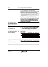
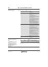
21.3.19 IEBus Receive
Interrupt Enable Register
(IEIER)
1131 Figure amended
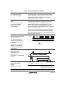
76543210
00000000
R/W R/W R/W R/W R/W R/W R/W R/W
Bit:
Initial value:
R/W:
RXBSYE RXSE RXFE RXEDEE
RXE
OVEE
RXE
RTMEE
RXE
DLEE
RXEPEE
22.4 Input/Output Pins
Table 22.1 Pin
Configuration
1153 Table amended
Channel Pin Name I/O Description
0 SPDIF_OUT Output Transmitter biphase-mark encoded SPDIF bitstream
1 SPDIF_IN Input Receiver biphase-mark encoded SPDIF bitstream