


Section 24 A/D Converter
Page 1276 of 2108 R01UH0134EJ0400 Rev. 4.00
Sep 24, 2014
SH7262 Group, SH7264 Group
24.4.4 A/D Converter Activation by External Trigger or Multi-Function Timer Pulse Unit
2
The A/D converter can be independently activated by an external trigger or an A/D conversion
request from the multi-function timer pulse unit 2. To activate the A/D converter by an external
trigger or the multi-function timer pulse unit 2, set the A/D trigger enable bits (TRGS[3:0]). When
an external trigger or an A/D conversion request from the multi-function timer pulse unit 2 is
generated with this bit setting, the ADST bit is set to 1 to start A/D conversion. The channel
combination is determined by bits CH2 to CH0 in ADCSR. The timing from setting of the ADST
bit until the start of A/D conversion is the same as when 1 is written to the ADST bit by software.
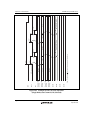
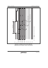
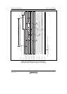
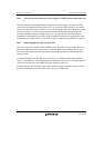
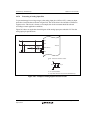
24.4.5 Input Sampling and A/D Conversion Time
The A/D converter has a built-in sample-and-hold circuit. The A/D converter samples the analog
input at the A/D conversion start delay time (t
D
) after the ADST bit in ADCSR is set to 1, then
starts conversion. Figure 24.5 shows the A/D conversion timing. Table 24.4 indicates the A/D
conversion time.
As indicated in figure 24.5, the A/D conversion time (t
CONV
) includes t
D
and the input sampling
time(t
SPL
). The length of t
D
varies depending on the timing of the write access to ADCSR. The total
conversion time therefore varies within the ranges indicated in table 24.4.
In multi mode and scan mode, the values given in table 24.4 apply to the first conversion. In the
second and subsequent conversions, time is the values given in table 24.5.