


Section 27 Video Display Controller 3
R01UH0134EJ0400 Rev. 4.00 Page 1613 of 2108
Sep 24, 2014
SH7262 Group, SH7264 Group
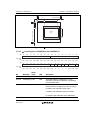
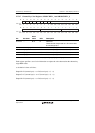
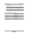
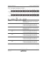
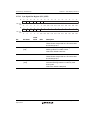
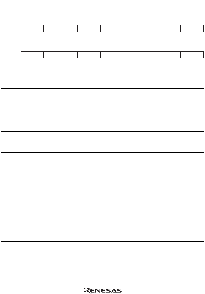
27.7.31 Sync Signal Control Register (SYNCNT)
31 30 29 28 27 26 25 24 23 22 21 20 19 18 17 16
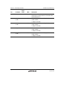
151413121110987654321
0
0000000000000000
RRRRRRRR/WRRRRR/WR/WR/WR/W
0000000000000000
RRRRRRRRRRRRR/WR/WR/WR/W
------
-
-
RGB_
TIM
----
VSYNC_
TIM
HSYNC_
TIM
DE_TIM
M_DISP
_TIM
----- ------
VSYNC
_TYPE
HSYNC
_TYPE
DE_
TYPE
M_DISP
_TYPE
Bit:
Initial value:
R/W:
Bit:
Initial value:
R/W:
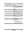
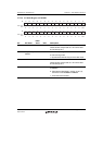
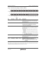
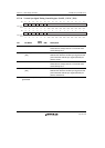
Bit Bit Name
Initial
Value R/W Description
31 to 25 All 0 R Reserved
These bits are always read as 0. The write value
should always be 0.
24 RGB_TIM 0 R/W Specifies the LCD_DATA output timing.
0: Output at the rising edge of the panel clock
1: Output at the falling edge of the panel clock
23 to 20 All 0 R Reserved
These bits are always read as 0. The write value
should always be 0.
19 VSYNC_
TIM
0 R/W Specifies the LCD_VSYNC output timing.
0: Output at the rising edge of the panel clock
1: Output at the falling edge of the panel clock
18 HSYNC_
TIM
0 R/W Specifies the LCD_HSYNC output timing.
0: Output at the rising edge of the panel clock
1: Output at the falling edge of the panel clock
17 DE_TIM 0 R/W Specifies the LCD_DE output timing.
0: Output at the rising edge of the panel clock
1: Output at the falling edge of the panel clock
16 M_DISP_
TIM
0 R/W Specifies the LCD_M_DISP output timing.
0: Output at the rising edge of the panel clock
1: Output at the falling edge of the panel clock