


Section 32 General Purpose I/O Ports
R01UH0134EJ0400 Rev. 4.00 Page 1689 of 2108
Sep 24, 2014
SH7262 Group, SH7264 Group
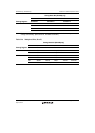
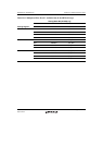
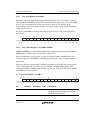
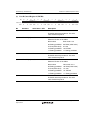
32.2.1 Port A I/O Register 0 (PAIOR0)
PAIOR0 is a 16-bit readable/writable register that is set the pins on port A as inputs or outputs.
The PA3IOR0 to PA0IOR bits correspond to the PA3 PA0 pins, respectively. If a bit in PAIOR0
is set to 1, the corresponding pin on port A functions as output. If it is cleared to 0, the
corresponding pin function as input. The direction (input or output) should only be modified by
writing once for each pin.
Bits 15 to 4 in PAIOR0 are reserved. These bits are always read as 0. The write value should
always be 0.
15 14 13 12 11 10 9 8 7 6 5 4 3 2 1 0
0000000000000000
R R R R R R R R R R R R R/W R/W R/W R/W
-----------
PA3
IOR
PA 2
IOR
PA1
IOR
PA0
IOR
-
Bit:
Initial value:
R/W:
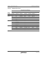
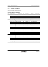
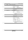
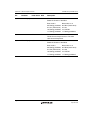
32.2.2 Port A Data Registers 1, 0 (PADR1, PADR0)
PBDR1 and PBDR0 are 16-bit readable/writable registers that store port A data. The PA3DR to
PA0DR bits correspond to the PA3 to PA0 pins, respectively.
When a pin function is general output, if a value is written to PADR1 or PADR0, that value is
output from the pin, and if PADR1 or PADR0 is read, the register value is returned regardless of
the pin state.
When a pin function is general input, if PADR1 or PADR0 is read, the pin state, not the register
value, is returned directly. If a value is written to PADR1 or PADR0, although that value is
written into PADR1 or PADR0, it does not affect the pin state. Table 32.13 summarizes PADR1
and PADR0 read/write operation.
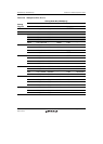
(1) Port A Data Register 1 (PADR1)
15 14 13 12 11 10 9 8 7 6 5 4 3 2 1 0
0000000000000000
RRRRRRRR/WRRRRRRRR/W
------
PA3
DR
-------
PA2
DR
-
Bit:
Initial value:
R/W:
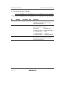
Bit Bit Name Initial Value R/W Description
15 to 9 All 0 R Reserved
These bits are always read as 0. The write
value should always be 0.