


Section 32 General Purpose I/O Ports
R01UH0134EJ0400 Rev. 4.00 Page 1725 of 2108
Sep 24, 2014
SH7262 Group, SH7264 Group
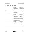
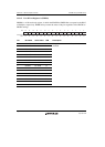
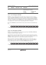
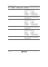
Bit Bit Name Initial Value R/W Description
1, 0 PE0MD[1:0] 00 R/W PE0 Mode
Select the function of the PE0.
00: PE0
01: SCL0
10: AUDIO_CLK
11: IRQ0
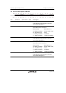
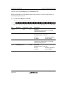
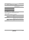
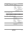
32.2.17 Port E I/O Register 0 (PEIOR0)
PEIOR0 is a 16-bit readable/writable register that is used to set the pins on port F as inputs or
outputs. The PE5IOR to PE0IOR bits correspond to the PE5 to PE0 pins respectively. PEIOR0 is
enabled when the port E pins are functioning as general-purpose inputs/outputs (PE5 to PE0). In
other states, it is disabled. If a bit in PEIOR0 is set to 1, the corresponding pin on port E functions
as an output pin. If it is cleared to 0, the corresponding pin functions as an input pin.
Bits 15 to 6 in PEIOR0 are reserved. This bit is always read as 0. The write value should always
be 0.
15 14 13 12 11 10 9 8 7 6 5 4 3 2 1 0
0000000 000000000
R R R R R R R R R R R/W R/W R/W R/W R/W R/W
--------
-
PE5
IOR
PE4
IOR
PE3
IOR
PE2
IOR
PE1
IOR
PE0
IOR
-
Bit:
Initial value:
R/W:
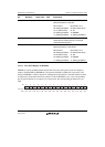
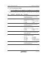
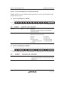
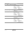
32.2.18 Port E Data Register 0 (PEDR0)
PEDR0 is a 16-bit readable/writable register that stores port E data. The PE5DR to PE0DR bits
correspond to the PE5 to PE0 pins, respectively.
6 pins on Port E are open-drain outputs. When a pin function is general output, if 0 is written to
PEDR0, 0 is output from the pin and if 1 is written to, the pin will be in the high-impedance state.
If PEDR0 is read, the register value is returned directly regardless of the pin state.
When a pin function is general input, if PEDR0 is read, the pin state, not the register value, is
returned directly. If a value is written to PEDR0, although that value is written into PEDR0, it
does not affect the pin state. Table 32.17 summarizes PEDR0 read/write operation.
15 14 13 12 11 10 9 8 7 6 5 4 3 2 1 0
0000000 000000000
RRRRRRRRRRR/WR/WR/WR/WR/WR/W
---------
PE5
DR
PE4
DR
PE3
DR
PE2
DR
PE1
DR
PE0
DR
-
Bit:
Initial value:
R/W: