


Section 11 Multi-Function Timer Pulse Unit 2
Page 548 of 2108 R01UH0134EJ0400 Rev. 4.00
Sep 24, 2014
SH7262 Group, SH7264 Group
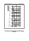
(d) PWM Output Level Setting
In complementary PWM mode, the PWM pulse output level is set with bits OLSN and OLSP in
timer output control register 1 (TOCR1) or bits OLS1P to OLS3P and OLS1N to OLS3N in timer
output control register 2 (TOCR2).
The output level can be set for each of the three positive phases and three negative phases of 6-
phase output.
Complementary PWM mode should be cleared before setting or changing output levels.
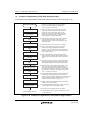
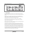
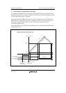
(e) Dead Time Setting
In complementary PWM mode, PWM pulses are output with a non-overlapping relationship
between the positive and negative phases. This non-overlap time is called the dead time.
The non-overlap time is set in the timer dead time data register (TDDR). The value set in TDDR is
used as the TCNT_3 counter start value, and creates non-overlap between TCNT_3 and TCNT_4.
Complementary PWM mode should be cleared before changing the contents of TDDR.
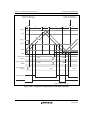
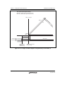
(f) Dead Time Suppressing
Dead time generation is suppressed by clearing the TDER bit in the timer dead time enable
register (TDER) to 0. TDER can be cleared to 0 only when 0 is written to it after reading TDER =
1.
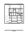
TGRA_3 and TGRC_3 should be set to 1/2 PWM carrier cycle + 1 and the timer dead time data
register (TDDR) should be set to 1.
By the above settings, PWM waveforms without dead time can be obtained. Figure 11.41 shows
an example of operation without dead time.