


Section 1 Overview
Page 20 of 2108 R01UH0134EJ0400 Rev. 4.00
Sep 24, 2014
SH7262 Group, SH7264 Group
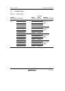
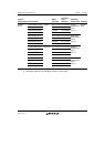
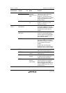
Classification Symbol I/O Name Function
Clock AUDIO_X1 I Crystal
resonator/
external clock for
audio
Pins connected to a crystal
resonator for audio. An external
clock can be input on pin
AUDIO_X1. A clock input to the
divider is selected from an oscillation
clock input on these pins or the
AUDIO_CLK pin.
AUDIO_X2 O
AUDIO_XOUT O AUDIO_X1 clock
I/O
Output for the on-chip crystal
oscillator on AUDIO_X1 or the
external clock signal.
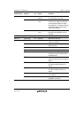
Operating mode
control
MD_BOOT1
MD_BOOT0
I Mode set Sets the operating mode. Do not
change the signal levels on these
pins while the RES pin is asserted or
until the mode is fixed, after the
negation.
MD_CLK1,
MD_CLK0
I Clock mode set These pins set the clock operating
mode. Do not change the signal
levels on these pins while the RES
pin is asserted or until the mode is
fixed, after the negation.
ASEMD I ASE mode If a low level is input at the ASEMD
pin while the RES pin is asserted,
ASE mode is entered; if a high level
is input, product chip mode is
entered.
In ASE mode, the E10A-USB
emulator function is enabled. When
this function is not in use, fix it high.
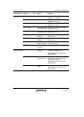
System control RES I Power-on reset This LSI enters the power-on reset
state when this signal goes low.
WDTOVF O Watchdog timer
overflow
Outputs an overflow signal from the
watchdog timer.
BREQ I Bus-mastership
request
A low level is input to this pin when
an external device requests the
release of the bus mastership.
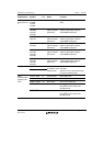
BACK O Bus-mastership
request
acknowledge
Indicates that the bus mastership
has been released to an external
device. Reception of the BACK
signal informs the device which has
output the BREQ signal that it has
acquired the bus.