


Section 9 Bus State Controller
R01UH0134EJ0400 Rev. 4.00 Page 367 of 2108
Sep 24, 2014
SH7262 Group, SH7264 Group
CPU performs four contiguous longword read cycles to perform cache fill operations via the
internal bus. If a cache miss occurs in byte or word operand access or at a branch to an odd word
boundary (4n + 2), the CPU performs four contiguous longword access cycles to perform a cache
fill operation on the external interface. For a cache-disabled space, the CPU performs access
according to the actual access addresses. For an instruction fetch to an even word boundary (4n),
the CPU performs longword access. For an instruction fetch to an odd word boundary (4n + 2), the
CPU performs word access.
For a read cycle of an on-chip peripheral module, the cycle is initiated through the internal bus and
peripheral bus. The read data is sent to the CPU via the peripheral bus, internal bus, and CPU bus.
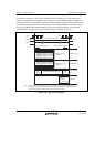
In a write cycle for the cache-enabled space, the write cycle operation differs according to the
cache write methods.
In write-back mode, the cache is first searched. If data is detected at the address corresponding to
the cache, the data is then re-written to the cache. In the actual memory, data will not be re-written
until data in the corresponding address is re-written. If data is not detected at the address
corresponding to the cache, the cache is modified. In this case, data to be modified is first saved to
the internal buffer, 16-byte data including the data corresponding to the address is then read, and
data in the corresponding access of the cache is finally modified. Following these operations, a
write-back cycle for the saved 16-byte data is executed.
In write-through mode, the cache is first searched. If data is detected at the address corresponding
to the cache, the data is re-written to the cache simultaneously with the actual write via the internal
bus. If data is not detected at the address corresponding to the cache, the cache is not modified but
an actual write is performed via the internal bus.
Since the bus state controller incorporates a one-stage write buffer, it can execute an access via the
internal bus before the previous external bus cycle is completed in a write cycle. If the on-chip
module is read or written after the external low-speed memory is written, the on-chip module can
be accessed before the completion of the external low-speed memory write cycle.
In read cycles, the CPU is placed in the wait state until read operation has been completed. To
continue the process after the data write to the device has been completed, perform a dummy read
to the same address to check for completion of the write before the next process to be executed.