


Section 9 Bus State Controller
Page 234 of 2108 R01UH0134EJ0400 Rev. 4.00
Sep 24, 2014
SH7262 Group, SH7264 Group
9.3 Area Overview
9.3.1 Address Map
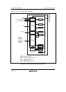
In the architecture, this LSI has a 32-bit address space, which is divided into cache-enabled,
cache-disabled, and on-chip spaces (on-chip RAM, on-chip peripheral modules, and reserved
areas) according to the upper bits of the address.
External address spaces CS0 to CS6 are cache-enabled when internal address A29 = 0 or cache-
disabled when A29 = 1.
The kind of memory to be connected and the data bus width are specified in each partial space.
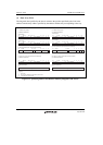
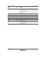
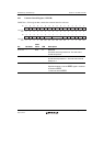
The address map for the external address space is listed below.
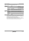
Table 9.2 Address Map
Internal Address Space Memory to be Connected Cache
H'00000000 to H'03FFFFFF CS0 Normal space, SRAM with byte selection,
burst ROM (asynchronous or synchronous)
Cache-enabled
H'04000000 to H'07FFFFFF CS1 Normal space, SRAM with byte selection
H'08000000 to H'0BFFFFFF CS2 Normal space, SRAM with byte selection,
SDRAM
H'0C000000 to H'0FFFFFFF CS3 Normal space, SRAM with byte selection,
SDRAM
H'10000000 to H'13FFFFFF CS4 Normal space, SRAM with byte selection,
burst ROM (asynchronous)
H'14000000 to H'17FFFFFF CS5 Normal space, SRAM with byte selection,
MPX-I/O, PCMCIA
H'18000000 to H'1BFFFFFF CS6 Normal space, SRAM with byte selection,
PCMCIA
H'1C000000 to H'1FFFFFFF Other On-chip RAM
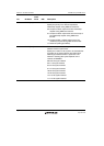
H'20000000 to H'23FFFFFF CS0 Normal space, SRAM with byte selection,
burst ROM (asynchronous or synchronous)
Cache-disabled
H'24000000 to H'27FFFFFF CS1 Normal space, SRAM with byte selection
H'28000000 to H'2BFFFFFF CS2 Normal space, SRAM with byte selection,
SDRAM
H'2C000000 to H'2FFFFFFF CS3 Normal space, SRAM with byte selection,
SDRAM
H'30000000 to H'33FFFFFF CS4 Normal space, SRAM with byte selection,
burst ROM (asynchronous)
H'34000000 to H'37FFFFFF CS5 Normal space, SRAM with byte selection,
MPX-I/O, PCMCIA