


Section 15 Serial Communication Interface with FIFO
Page 772 of 2108 R01UH0134EJ0400 Rev. 4.00
Sep 24, 2014
SH7262 Group, SH7264 Group
15.6.3 Restriction on Direct Memory Controller Usage
When the direct memory access controller writes data to SCFTDR due to a TXI interrupt request,
the state of the TEND flag becomes undefined. Therefore, the TEND flag should not be used as
the transfer end flag in such a case.
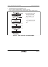
15.6.4 Break Detection and Processing
Break signals can be detected by reading the RxD pin directly when a framing error (FER) is
detected. In the break state the input from the RxD pin consists of all 0s, so the FER flag is set and
the parity error flag (PER) may also be set.
Note that, although transfer of receive data to SCFRDR is halted in the break state, the receive
operation is continued.
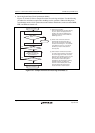
15.6.5 Sending a Break Signal
The I/O condition and level of the TxD pin are determined by the SPB2IO and SPB2DT bits in the
serial port register (SCSPTR). This feature can be used to send a break signal.
Until TE bit is set to 1 (enabling transmission) after initializing, the TxD pin does not work.
During the period, mark status is performed by the SPB2DT bit. Therefore, the SPB2IO and
SPB2DT bits should be set to 1 (high level output).
To send a break signal during serial transmission, clear the SPB2DT bit to 0 (designating low
level), then clear the TE bit to 0 (halting transmission). When the TE bit is cleared to 0, the
transmitter is initialized regardless of the current transmission state, and 0 is output from the TxD
pin.
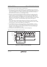
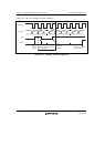
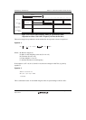
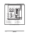
15.6.6 Receive Data Sampling Timing and Receive Margin (Asynchronous Mode)
This module operates on a base clock with a frequency 16 or 8 times the bit rate. In reception, the
falling edge of the start bit is sampled at the base clock to perform synchronization internally.
Receive data is latched at the rising edge of the eighth or fourth base clock pulse. When this
module operates on a base clock with a frequency 16 times the bit rate, the receive data is sampled
at the timing shown in figure 15.19.