


Section 9 Bus State Controller
Page 336 of 2108 R01UH0134EJ0400 Rev. 4.00
Sep 24, 2014
SH7262 Group, SH7264 Group
(12) Power-On Sequence
In order to use SDRAM, mode setting must first be made for SDRAM after the pose interval
specified for the SDRAM to be used after powering on. The pose interval should be obtained by a
power-on reset generating circuit or software.
To perform SDRAM initialization correctly, the registers of this module must first be set, followed
by a write to the SDRAM mode register. In SDRAM mode register setting, the address signal
value at that time is latched by a combination of the CSn, RAS, CAS, and RD/WR signals. If the
value to be set is X, the bus state controller provides for value X to be written to the SDRAM
mode register by performing a word write to address H'FFFC4000 + X for area 2 SDRAM, and to
address H'FFFC5000 + X for area 3 SDRAM. In this operation the data is ignored, but the mode
write is performed as a byte-size access. To set burst read/single write or burst read/burst write
(CAS latency 2 to 3, wrap type = sequential, and burst length 1) supported by the LSI, arbitrary
data is written in a byte-size access to the addresses shown in table 9.13. In this time 0 is output at
the external address pins of A12 or later.
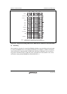
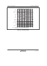
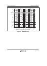
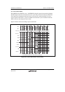
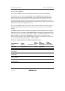
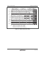
Table 9.13 Access Address in SDRAM Mode Register Write
Setting for Area 2
Burst read/single write (burst length 1):
Data Bus Width CAS Latency Access Address External Address Pin
16 bits 2 H'FFFC4440 H'0000440
3 H'FFFC4460 H'0000460
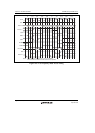
Burst read/burst write (burst length 1):
Data Bus Width CAS Latency Access Address External Address Pin
16 bits 2 H'FFFC4040 H'0000040
3 H'FFFC4060 H'0000060