


Page 2080 of 2108 R01UH0134EJ0400 Rev. 4.00
Sep 24, 2014
Item Page Revision (See Manual for Details)
23.6.3 Link Blocks 1257 Description amended
Perform the following processing for seven sectors
(indicated by ISEC being generated seven times) after
finding that the LINK_OUT1 bit has been set to 1.
...
Forcibly stop decoding, set the CROMSY0 register to
place the decoder in external sync mode, and retry
decoding by specifying the MSF value stored above + 7
as the MSF value for the target sector. The start sector
address will be the address where RUN_OUT is stored
+ 7 .
24.7.7 A/D Conversion in
Deep Standby Mode
1285 Section deleted
26.1 Features
(5) Pipe Configuration
1344 Description amended
Transfer conditions that can be set for each pipe:
PIPE0: Control transfer (default control pipe: DCP),
256-byte fixed single buffer
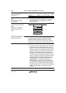
26.3.1 System
Configuration Control
Register (SYSCFG)
1353 Table amended
Bit Bit Name
Initial
Value
R/W Description
0 USBE 0 R/W USB Module Operation Enable
...
When the host controller function is selected, this bit
should be set to 1 after setting DRPD to 1, eliminating
LNST bit chattering, and checking that the USB bus
has been settled.
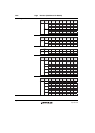
26.3.5 Test Mode Register
(TESTMODE)
1363 Table amended
Bit Bit Name
Initial
Value
R/W Description
3 to 0 UTST[3:0] 0000 R/W (1) When the host controller function is selected
These bits can be set after writing 1 to DRPD. This
module outputs waveforms when both DRPD and
UACT are set to 1. This module also performs high-
speed termination after the UTST bits are written to.
• Procedure for setting the UTST bits
1. Power-on reset.
2. Start the clock supply (Set SCKE to 1 after
the crystal oscillation and the PLL for USB
are settled).
3. Set DCFM and DRPD to 1 (setting HSE to 1
is not required).
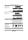
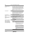
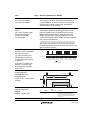
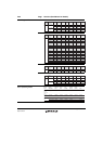
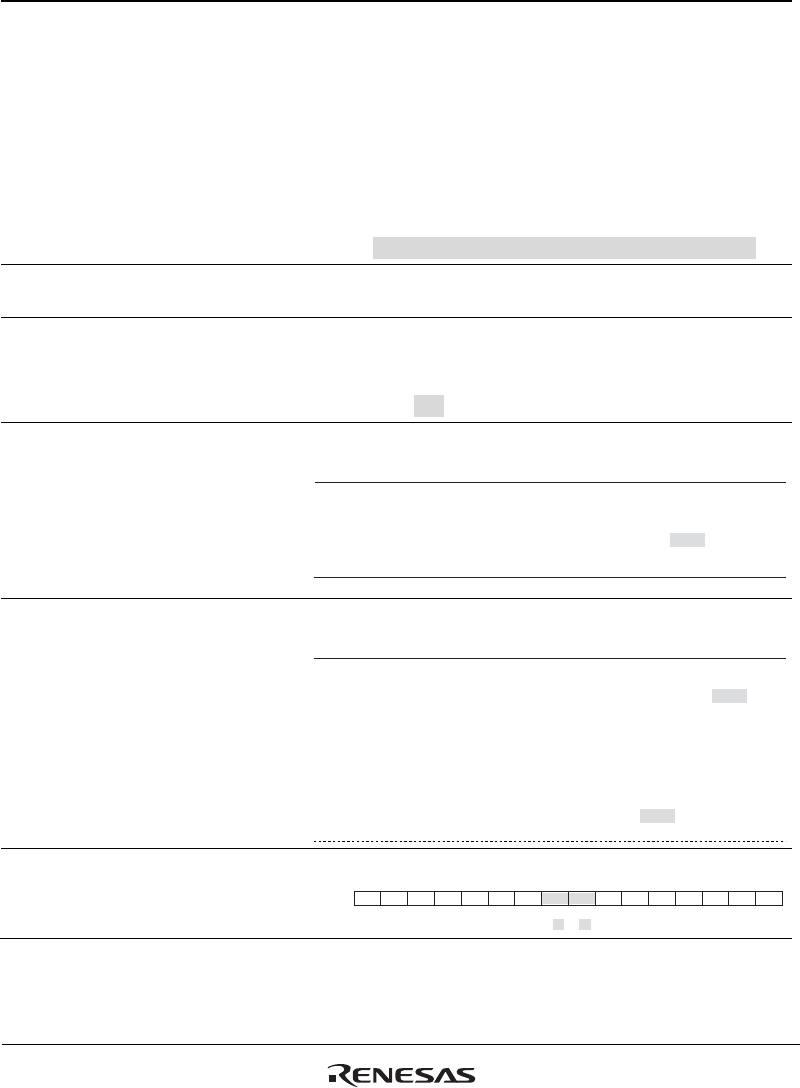
26.3.28 DCP Configuration
Register (DCPCFG)
1415 Figure amended
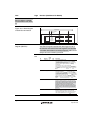
15 14 13 12 11 10 9 8 76543210
Bit:
Initial value:
R/W:
0000000000000000
RRRRRRRR/WR/WRRR/WRRRR
———————CNTMD
SHTNAK
——DIR————