


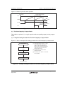
Section 11 Multi-Function Timer Pulse Unit 2
R01UH0134EJ0400 Rev. 4.00 Page 517 of 2108
Sep 24, 2014
SH7262 Group, SH7264 Group
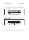
(2) Examples of Buffer Operation
(a) When TGR is an output compare register
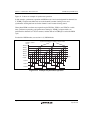
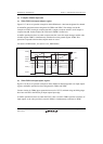
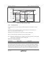
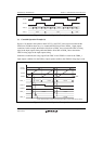
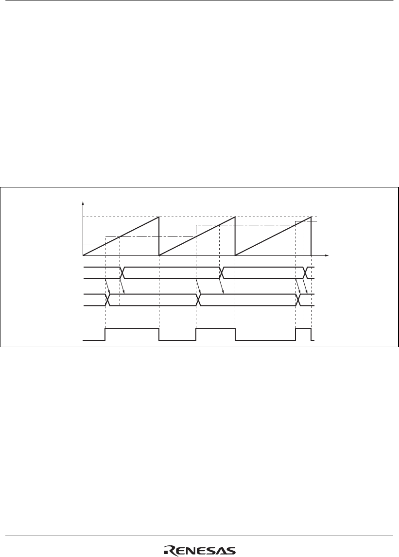
Figure 11.17 shows an operation example in which PWM mode 1 has been designated for channel
0, and buffer operation has been designated for TGRA and TGRC. The settings used in this
example are TCNT clearing by compare match B, 1 output at compare match A, and 0 output at
compare match B. In this example, the TTSA bit in TBTM is cleared to 0.
As buffer operation has been set, when compare match A occurs the output changes and the value
in buffer register TGRC is simultaneously transferred to timer general register TGRA. This
operation is repeated each time that compare match A occurs.
For details of PWM modes, see section 11.4.5, PWM Modes.
TCNT value
TGRB_0
H'0000
TGRC_0
TGRA_0
H'0200 H'0520
TIOCA
H'0200
H'0450
H'0520
H'0450
TGRA_0
H'0450
H'0200
Transfer
Time
Figure 11.17 Example of Buffer Operation (1)
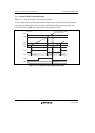
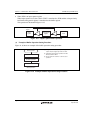
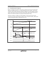
(b) When TGR is an input capture register
Figure 11.18 shows an operation example in which TGRA has been designated as an input capture
register, and buffer operation has been designated for TGRA and TGRC.
Counter clearing by TGRA input capture has been set for TCNT, and both rising and falling edges
have been selected as the TIOCA pin input capture input edge.
As buffer operation has been set, when the TCNT value is stored in TGRA upon the occurrence of
input capture A, the value previously stored in TGRA is simultaneously transferred to TGRC.