


Section 37 Electrical Characteristics
R01UH0134EJ0400 Rev. 4.00 Page 1975 of 2108
Sep 24, 2014
SH7262 Group, SH7264 Group
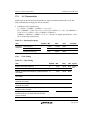
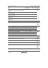
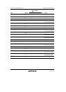
Item Symbol Min. Max. Unit Figure
USB_X1 clock input frequency (when neither high-
speed transfer function nor host controller function
is used)
fEX 48 MHz 2500 ppm Figure
37.1
EXTAL, AUDIO_X1, AUDIO_CLK, USB_X1 clock
input low pulse width
tEXL 0.4 0.6 t
EXcyc
EXTAL, AUDIO_X1, AUDIO_CLK, USB_X1 clock
input high pulse width
tEXH 0.4 0.6 t
EXcyc
EXTAL, AUDIO_X1, AUDIO_CLK, USB_ X1 clock
input rise time
tEXr 4 ns
EXTAL, AUDIO_X1, AUDIO_CLK, USB_ X1 clock
input fall time
tEXf 4 ns
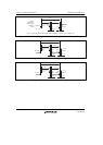
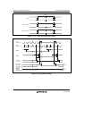
CKIO clock output frequency fOP 40.00 72.00 MHz
CKIO clock output cycle time tcyc 13.88 25 ns Figures
37.2 (1)
and
37.2 (2)
CKIO clock output low pulse width 1 tCKOL1 t
cyc
/2 tCKOr1 ns Figure
37.2 (1)
CKIO clock output high pulse width 1 tCKOH1 t
cyc
/2 tCKOr1 ns
CKIO clock output rise time 1 tCKOr1 3 ns
CKIO clock output fall time 1 tCKOf1 3 ns
CKIO clock output low pulse width 2 tCKOL2 t
cyc
/2 tCKOr2 ns Figure
37.2 (2)
CKIO clock output high pulse width 2 tCKOH2 t
cyc
/2 tCKOr2 ns
CKIO clock output rise time 2 tCKOr2 2 ns
CKIO clock output fall time 2 tCKOf2 2 ns
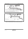
Power-on oscillation settling time tOSC1 10 ms Figure
37.3
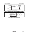
Oscillation settling time 1 on return from standby tOSC2 10 ms Figure
37.4
Oscillation settling time 2 on return from standby tOSC3 10 ms Figure
37.5
Real time clock oscillation settling time tROSC 3 s Figure
37.6
Mode hold time tMDH 200 ns Figures
37.3
and
37.4