


Section 33 Power-Down Modes
R01UH0134EJ0400 Rev. 4.00 Page 1795 of 2108
Sep 24, 2014
SH7262 Group, SH7264 Group
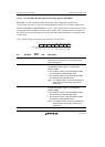
Bit Bit Name
Initial
Value R/W Description
7 to 4 All 0 R Reserved
These bits are always read as 0. The write value
should always be 0.
3 RRAMWE3 0 R/W RAM Write Enable 3 (corresponding area: page 3*
3
*
4
in on-chip data-retention RAM)
0: Writing to page 3 is disabled.
1: Writing to page 3 is enabled.
2 RRAMWE2 0 R/W RAM Write Enable 2 (corresponding area: page 2*
2
in
on-chip data-retention RAM
0: Writing to page 2 is disabled.
1: Writing to page 2 is enabled.
1 RRAMWE1 0 R/W RAM Write Enable 1 (corresponding area: page 1*
2
in
on-chip data-retention RAM
0: Writing to page 1 is disabled.
1: Writing to page 1 is enabled.
0 RRAMWE0 0 R/W RAM Write Enable 0 (corresponding area: page 0*
2
in
on-chip data-retention RAM)
0: Writing to page 0 is disabled.
1: Writing to page 0 is enabled.
Notes: 1. For addresses in each page, see section 31, On-Chip RAM.
2. When the VRAME0 bit in SYSCR3 is cleared to 0 (access to page 0 in large-capacity
on-chip RAM is invalid), the on-chip data-retention RAM cannot be accessed (read and
written), regardless of the setting of this bit.
When the VRAMWE0 bit in SYSCR4 is cleared to 0 (writing to page 0 in large-capacity
on-chip RAM is invalid), the on-chip data-retention RAM cannot be written, regardless
of the setting of this bit.
3. When the VRAME1 bit in SYSCR3 is cleared to 0 (access to page 1 in large-capacity
on-chip RAM is invalid), the first half (page 1 in large-capacity on-chip RAM) of the on-
chip data-retention RAM cannot be accessed (read and written), regardless of the
setting of this bit.
When the VRAME1 bit in SYSCR4 is cleared to 0 (writing to page 1 in large-capacity
on-chip RAM is invalid), the first half of the on-chip data-retention RAM cannot be
written, regardless of the setting of this bit.
4. When the VRAME2 bit in SYSCR3 is cleared to 0 (access to page 2 in large-capacity
on-chip RAM is invalid), the second half (page 2 in large-capacity on-chip RAM) of the
on-chip data-retention RAM cannot be accessed (read and written), regardless of the
setting of this bit.
When the VRAMWE2 bit in SYSCR4 is cleared to 0 (writing to page 2 in large-capacity
on-chip RAM is invalid), the second half of the on-chip data-retention RAM cannot be
written, regardless of the setting of this bit.