


Section 9 Bus State Controller
Page 362 of 2108 R01UH0134EJ0400 Rev. 4.00
Sep 24, 2014
SH7262 Group, SH7264 Group
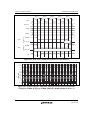
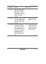
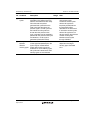
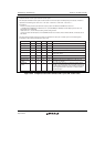
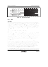
Table 9.19 Number of Idle Cycles Inserted between Access Cycles to Different Memory
Types
Next Cycle
Previous Cycle SRAM
Burst ROM
(Asynchronous)
MPX-
I/O
Byte
SRAM
(BAS = 0)
Byte
SRAM
(BAS = 1) SDRAM
SDRAM
(Low-
Frequency
Mode) PCMCIA
Burst ROM
(Synchronous)
SRAM 0 0 1 0 0/1*
1
0/1*
1
1.5 0 0
Burst ROM
(asynchronous)
0 0 1 0 0/1*
1
0/1*
1
1.5 0 0
MPX-I/O 1 1 0 1 1 1 1.5 1 1
Byte SRAM
(BAS = 0)
0 0 1 0 0/1*
1
0/1*
1
1.5 0 0
Byte SRAM
(BAS = 1)
0/1*
1
0/1*
1
1/2*
1
0/1*
1
0 0 1.5 0/1*
1
0/1*
1
SDRAM 1 1 2 1 0 0 1 1
SDRAM
(low-frequency
mode)
1.5 1.5 2.5 1.5 0.5 1 1.5 1.5
PCMCIA 0 0 1 0 0/1*
2
0/1*
2
1.5 0 0
Burst ROM
(synchronous)
0 0 1 0 1 1 1.5 0 0
Notes: 1. The number of idle cycles is determined by the setting of the CSnWCR.HW[1:0] bits on
the previous cycle. The number of idle cycles will be the number shown at the left when
HW[1:0] B'00, will be the number shown at the right when HW[1:0] = B'00. Also, for
CSn spaces for which the CSnWCR.HW[1:0] bits do not exist, the number of idle cycles
shown at the right will be used.
2. The number of idle cycles is determined by the setting of the CSnWCR.TEH[3:0] bits on
the previous cycle. The number of idle cycles will be the number shown at the left when
TEH[3:0] B'0000, will be the number shown at the right when TEH[3:0] = B'0000.
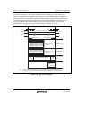
Figure 9.46 shows sample estimation of idle cycles between access cycles. In the actual operation,
the idle cycles may become shorter than the estimated value due to the write buffer effect or may
become longer due to internal bus idle cycles caused by stalling in the pipeline due to CPU
instruction execution or CPU register conflicts. Please consider these errors when estimating the
idle cycles.