


Section 17 I
2
C Bus Interface 3
R01UH0134EJ0400 Rev. 4.00 Page 871 of 2108
Sep 24, 2014
SH7262 Group, SH7264 Group
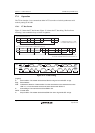
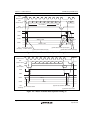
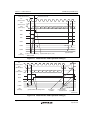
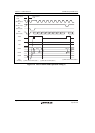
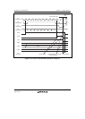
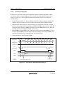
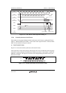
17.4.3 Master Receive Operation
In master receive mode, the master device outputs the receive clock, receives data from the slave
device, and returns an acknowledge signal. For master receive mode operation timing, refer to
figures 17.7 and 17.8. The reception procedure and operations in master receive mode are shown
below.
1. Clear the TEND bit in ICSR to 0, then clear the TRS bit in ICCR1 to 0 to switch from master
transmit mode to master receive mode. Then, clear the TDRE bit to 0.
2. When ICDRR is read (dummy data read), reception is started, and the receive clock is output,
and data received, in synchronization with the internal clock. The master device outputs the
level specified by ACKBT in ICIER to SDA, at the 9th receive clock pulse.
3. After the reception of first frame data is completed, the RDRF bit in ICSR is set to 1 at the rise
of 9th receive clock pulse. At this time, the receive data is read by reading ICDRR, and RDRF
is cleared to 0.
4. The continuous reception is performed by reading ICDRR every time RDRF is set. If 8th
receive clock pulse falls after reading ICDRR by the other processing while RDRF is 1, SCL is
fixed low until ICDRR is read.
5. If next frame is the last receive data, set the RCVD bit in ICCR1 to 1 before reading ICDRR.
This enables the issuance of the stop condition after the next reception.
6. When the RDRF bit is set to 1 at rise of the 9th receive clock pulse, issue the stage condition.
7. When the STOP bit in ICSR is set to 1, read ICDRR. Then clear the RCVD bit to 0.
8. The operation returns to the slave receive mode.
Note: If only one byte is received, read ICDRR (dummy-read) after the RCVD bit in ICCR1 is
set.