


Section 9 Bus State Controller
R01UH0134EJ0400 Rev. 4.00 Page 235 of 2108
Sep 24, 2014
SH7262 Group, SH7264 Group
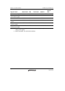
Internal Address Space Memory to be Connected Cache
H'38000000 to H'3BFFFFFF CS6 Normal space, SRAM with byte selection,
PCMCIA
Cache-disabled
H'3C000000 to H'3FFFFFFF Other On-chip RAM
H'40000000 to H'FFFBFFFF Other On-chip RAM, reserved area*
H'FFFC0000 to H'FFFFFFFF Other On-chip peripheral modules, reserved area*
Note: * For the on-chip RAM space, access the addresses shown in section 31, On-Chip RAM.
For the on-chip peripheral module space, access the addresses shown in section 36,
List of Registers. Do not access addresses which are not described in these sections.
Otherwise, the correct operation cannot be guaranteed.
9.3.2 Data Bus Width and Endian Specification of Each Area and Related Pin Settings
Depending on Boot Mode
The initial state of data bus, endian specification, and settings of the pins related to this module
depends on boot mode. For boot mode, refer to section 4, Boot Mode.
In boot mode 0, the state of area 0 is fixed to the state with bus width of 16 bits and big endian,
because this LSI is started up by the program stored in the ROM connected to area 0. The initial
state of areas 1 to 6 is the same as that of area 0, but the bus width and endian specification can be
changed by a program.
In this mode, settings required to read the ROM in area 0, such as settings for some of the
addresses, the data bus, and the pin functions of CS0 and RD only, are selected automatically
immediately after a power-on reset, but the initial function settings of the other pins are as general
ports. These pins cannot be used until their functions are set by a program. Do not perform other
than read access to area 0 until the pin settings are completed.
In boot modes 1 to 3, the state of areas 0 to 6 can be changed from the initial state by the program,
because in these modes the LSI is started by the program stored in the NAND flash memory or the
serial flash memory. Since pin functions related to this module are not set automatically, they need
to be set by the user. Do not access the external address space until the pin settings are completed.
Table 9.3 shows the initial state of areas 0 to 6 in boot mode 0, 2, and 3.
The sample access waveforms shown in this section include the pins such as BS, RD/WR, and
WEn. They are the waveforms when pin functions are assigned to the general I/O ports. When 8-
bit bus width is used, setting for pin A0 is also needed.
For details on pin function settings, see section 32, General Purpose I/O Ports.