


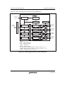

Section 34 User Debugging Interface
R01UH0134EJ0400 Rev. 4.00 Page 1825 of 2108
Sep 24, 2014
SH7262 Group, SH7264 Group
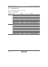
34.4.2 Reset Configuration
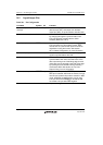
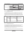
Table 34.5 Reset Configuration
ASEMD*
1
RES TRST Chip State
H L L Power-on reset and the reset of this module
H Power-on reset
H L Reset this module only
H Normal operation
L L L Reset hold*
2
H Power-on reset
H L Reset this module only
H Normal operation
Notes: 1. Performs product chip mode and ASE mode settings
ASEMD = H, normal mode
ASEMD = L, ASE mode
2. In ASE mode, reset hold is entered if the TRST pin is driven low while the RES pin is
negated. In this state, the CPU does not start up. When TRST is driven high, the
operation of this module is enabled, but the CPU does not start up. The reset hold state
is cancelled by a power-on reset.
34.4.3 TDO Output Timing
When the emulation command is enabled, a transition on the TDO pin is output on the falling edge
of TCK with the initial value. However, setting a TDO transition timing switching command in
SDIR via the pin and passing the Update-IR state synchronizes the TDO transition with the rising
edge of TCK.
To synchronize the transition of TDO with the falling edge of TCK after setting the TDO
transition timing switching command, the TRST pin must be asserted simultaneously with the
power-on reset. In the case of power-on reset by the RES pin, the sync reset is still in operation for
a certain period in the LSI even after the RES pin is negated. Thus, if the TRST pin is asserted
immediately after the negation of the RES pin, the TDO transition timing switching command is
cleared, resulting in TDO transitions synchronized with the falling edges of TCK. To prevent this,
make sure to allow a period of 20 tcyc or longer between the signal transitions of the RES and
TRST pins.