


Section 25 NAND Flash Memory Controller
R01UH0134EJ0400 Rev. 4.00 Page 1313 of 2108
Sep 24, 2014
SH7262 Group, SH7264 Group
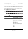
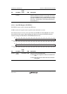
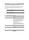
Bit Bit Name
Initial
Value R/W Description
19 to 0 RBTIMCN
T[19:0]
H'00000 R Ready Busy Timeout Counter
When the FRB pin is placed in a busy state, the values
of the bits RBTMOUT[19:0] in FLBSYTMR are copied to
these bits. These bits are counted down while the FRB
pin is busy. A timeout error occurs when these bits are
decremented to 0.
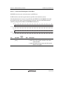
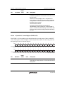
25.3.11 Data FIFO Register (FLDTFIFO)
FLDTFIFO is used to read or write the data FIFO area.
In DMA transfer, this register must be specified as the destination or source.
Note that the direction of read or write specified by the SELRW bit in FLCMDCR must match
that specified in this register. When changing the read/write direction, FLDTFIFO should be
cleared by setting the AC0CLR bit in FLINTDMACR before use.
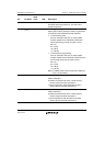
Bit:
Initial value:
R/W:
Bit:
Initial value:
R/W:
31 30 29 28 27 26 25 24 23 22 21 20 19 18 17 16
151413121110987654321
0
Undefined Undefined Undefined Undefined Undefined Undefined Undefined Undefined Undefined Undefined Undefined Undefined Undefined Undefined Undefined Undefined
R/W R/W R/W R/W R/W R/W R/W R/W R/W R/W R/W R/W R/W R/W R/W R/W
Undefined Undefined Undefined Undefined Undefined Undefined Undefined Undefined Undefined Undefined Undefined Undefined Undefined Undefined Undefined Undefined
R/W R/W R/W R/W R/W R/W R/W R/W R/W R/W R/W R/W R/W R/W R/W R/W
DTFO[31:16]
DTFO[15:0]
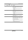
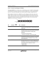
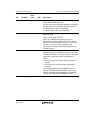
Bit Bit Name
Initial
Value
R/W Description
31 to 0 DTFO
[31:0]
H'xxxxxxxx R/W Data FIFO Area Read/Write Data
In write: Data in this register is written to the data FIFO
area.
In read: Data read from the data FIFO area is stored in
this register.