


Section 9 Bus State Controller
Page 348 of 2108 R01UH0134EJ0400 Rev. 4.00
Sep 24, 2014
SH7262 Group, SH7264 Group
This LSI
A16
.
.
.
A1
CSn
RD
RD/WR
D15
.
.
.
D0
WE1
WE0
A15
.
.
.
A0
CS
OE
WE
I/O 15
.
.
.
I/O 0
UB
LB
64K × 16-bit
SRAM
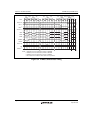
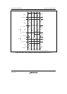
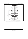
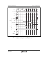
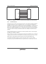
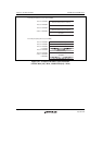
Figure 9.37 Example of Connection with 16-Bit Data-Width SRAM with Byte Selection
9.5.9 PCMCIA Interface
With this LSI, areas 5 and 6 can be used for the IC memory card and I/O card interface defined in
the JEIDA specifications version 4.2 (PCMCIA2.1 Rev. 2.1) by specifying bits TYPE[2:0] in
CSnBCR (n = 5 and 6) to B'101. In addition, the bits SA[1:0] in CSnWCR (n = 5 and 6) assign the
upper or lower 32 Mbytes of each area to IC memory card or I/O card interface. For example, if
the bits SA1 and SA0 in CS5WCR are set to 1 and cleared to 0, respectively, the upper 32 Mbytes
of area 5 are used for IC memory card interface and the lower 32 Mbytes are used for I/O card
interface.
When the PCMCIA interface is used, the bus size must be specified as 8 bits or 16 bits using the
bits BSZ[1:0] in CS5BCR or CS6BCR.
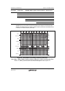
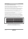
Figure 9.38 shows an example of connection between this LSI and a PCMCIA card. To enable hot
swapping (insertion and removal of the PCMCIA card with the system power turned on), tri-state
buffers must be connected between the bus interface of this LSI and the PCMCIA card.
In the JEIDA and PCMCIA standards, operation in big endian mode is not clearly defined.
Consequently, the provided PCMCIA interface in big endian mode is available only for this LSI.