


Section 33 Power-Down Modes
R01UH0134EJ0400 Rev. 4.00 Page 1789 of 2108
Sep 24, 2014
SH7262 Group, SH7264 Group
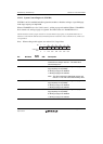
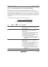
33.2.10 System Control Register 1 (SYSCR1)
SYSCR1 is an 8-bit readable/writable register that enables or disables access (read and write) to a
specified page in the high-speed on-chip RAM.
When an RAMEn (n = 0 to 3) bit is set to 1, access to page n is enabled. When an RAMEn bit is
cleared to 0, page n cannot be accessed. In this case, an undefined value is returned when reading
data or fetching an instruction from page n, and writing to page n is ignored. The initial value of
an RAMEn bit is 1.
Note that when clearing the RAMEn bit to 0, be sure to execute an instruction to read from or
write to the same arbitrary address in each page before setting the RAMEn bit. If such an
instruction is not executed, the data last written to page n may not be written to the high-speed on-
chip RAM.
SYSCR1 should be set with a program located in an area other than the high-speed on-chip RAM. Furthermore, an
instruction to read SYSCR1 should be located immediately after the instruction to write to SYSCR1. If not, normal access
is not guaranteed.
Note: When writing to this register, see section 33.4, Usage Notes.
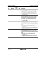
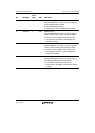
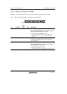
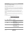
76543210
Bit:
Initial value:
R/W:
11111111
R R R R R/W R/W R/W R/W
----RAME3RAME2RAME1RAME0
Bit Bit Name
Initial
Value R/W Description
7 to 4 All 1 R Reserved
These bits are always read as 1. The write value
should always be 1.
3 RAME3 1 R/W RAM Enable 3 (corresponding area: page 3* in high-
speed on-chip RAM)
0: Access to page 3 is disabled.
1: Access to page 3 is enabled.
2 RAME2 1 R/W RAM Enable 2 (corresponding area: page 2* in high-
speed on-chip RAM)
0: Access to page 2 is disabled.
1: Access to page 2 is enabled.