Section 9 Bus State Controller
Page 328 of 2108 R01UH0134EJ0400 Rev. 4.00
Sep 24, 2014
SH7262 Group, SH7264 Group
TpwTp Tc1Tr
CKIO
A25 to A0
CS3
RD/WR
RAS
DQMx
D15 to D0
BS
DACKn*
2
A12/A11*
1
CAS
Notes: 1. Address pin to be connected to pin A10 of SDRAM.
2. The waveform for DACKn is when active low is specified.
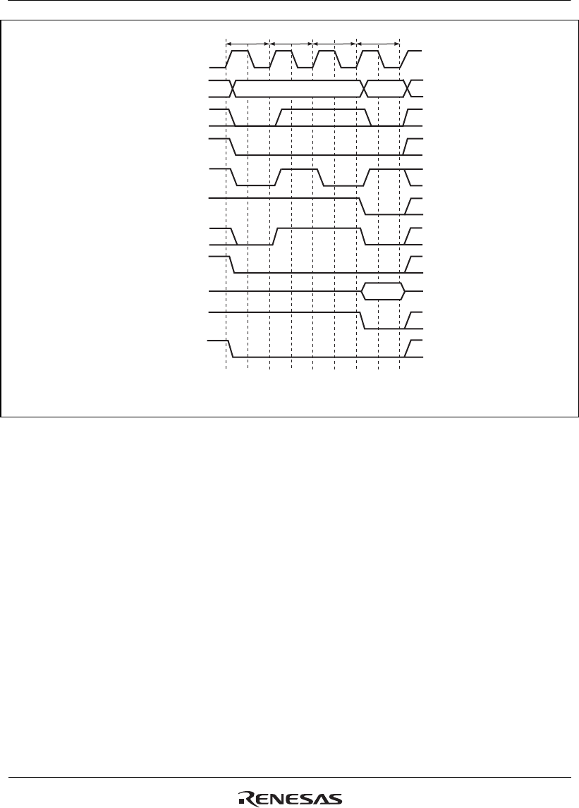
Figure 9.25 Single Write Timing (Bank Active, Different Row Addresses in the Same Bank)
(8) Refreshing
This module has a function for controlling SDRAM refreshing. Auto-refreshing can be performed
by clearing the RMODE bit to 0 and setting the RFSH bit to 1 in SDCR. A continuous refreshing
can be performed by setting the RRC2 to RRC0 bits in RTCSR. If SDRAM is not accessed for a
long period, self-refresh mode, in which the power consumption for data retention is low, can be
activated by setting both the RMODE bit and the RFSH bit to 1.


