


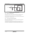

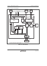

Section 25 NAND Flash Memory Controller
R01UH0134EJ0400 Rev. 4.00 Page 1289 of 2108
Sep 24, 2014
SH7262 Group, SH7264 Group
(6) Data Error
When a program error or erase error occurs, the error is reflected on the error source flags.
Interrupts for each source can be specified.
When a read error occurs, an ECC in the control code is other than 0. This read error is
reflected on the ECC error source flag.
When an ECC error occurs, perform an error correction, specify another sector to be replaced,
and copy the contents of the block to another sector as required.
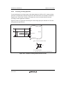
(7) Data Transfer FIFO and Data Register
The 224-byte data FIFO register (FLDTFIFO) is incorporated for data transfer of flash
memory.
The 32-byte control code FIFO register (FLECFIFO) is incorporated for data transfer of
control code.
(8) DMA Transfer
By individually specifying the destinations of data and control code of flash memory to the
direct memory access controller, data and control code can be sent to different areas.
(9) Access Time
The operating clock (FCLK) on the pins for the NAND-type flash memory is generated by
dividing the peripheral clock (P). The division ratio can be specified by the QTSEL bit in the
common control register (FLCMNCR).
Before changing the clock pulse generator configuration, this module must be placed in a
module stop state.
In NAND-type flash memory, the FRE and FWE pins operate at the frequency of FCLK. The
operating frequency must be specified within the maximum operating frequency of memory to
be connected.