


Section 15 Serial Communication Interface with FIFO
Page 752 of 2108 R01UH0134EJ0400 Rev. 4.00
Sep 24, 2014
SH7262 Group, SH7264 Group
(2) Clock
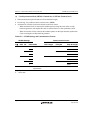
An internal clock generated by the on-chip baud rate generator or an external clock input from the
SCK pin can be selected as the transmit/receive clock. The clock source is selected by the C/A bit
in the serial mode register (SCSMR) and the CKE1 and CKE0 bits in the serial control register
(SCSCR). For clock source selection, refer to table 15.10, SCSMR and SCSCR Settings and Clock
Source Selection.
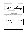
When an external clock is input at the SCK pin, it must have a frequency equal to 16 or 8 times
the desired bit rate.
When this module operates on an internal clock, it can output a clock signal on the SCK pin. The
frequency of this output clock is 16 or 8 times the desired bit rate.
(3) Transmitting and Receiving Data
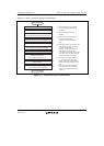
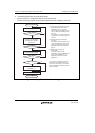
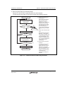
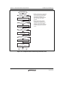
Initialization (Asynchronous Mode)
Before transmitting or receiving, clear the TE and RE bits to 0 in the serial control register
(SCSCR), then initialize this module as follows.
When changing the operation mode or the communication format, always clear the TE and RE
bits to 0 before following the procedure given below. Clearing TE to 0 initializes the transmit
shift register (SCTSR). Clearing TE and RE to 0, however, does not initialize the serial status
register (SCFSR), transmit FIFO data register (SCFTDR), or receive FIFO data register
(SCFRDR), which retain their previous contents. Clear TE to 0 after all transmit data has been
transmitted and the TEND flag in the SCFSR is set. The TE bit can be cleared to 0 during
transmission, but the transmit data goes to the Mark state after the bit is cleared to 0. Set the
TFRST bit in SCFCR to 1 and reset SCFTDR before TE is set again to start transmission.
When an external clock is used, the clock should not be stopped during initialization or
subsequent operation. The operation becomes unreliable if the clock is stopped.