


Section 9 Bus State Controller
Page 306 of 2108 R01UH0134EJ0400 Rev. 4.00
Sep 24, 2014
SH7262 Group, SH7264 Group
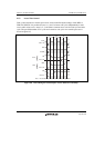
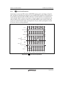
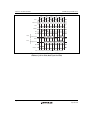
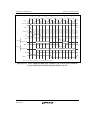
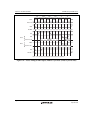
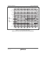
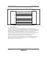
9.5.6 SDRAM Interface
(1) SDRAM Direct Connection
The SDRAM that can be connected to this LSI is a product that has 11/12/13 bits of row address,
8/9/10 bits of column address, 4 or less banks, and uses the A10 pin for setting precharge mode in
read and write command cycles.
The control signals for direct connection of SDRAM are RAS, CAS, RD/WR, DQMU, DQML,
CKE, CS2, and CS3. All the signals other than CS2 and CS3 are common to all areas, and signals
other than CKE are valid only when CS2 or CS3 is asserted. SDRAM can be connected to up to 2
spaces. The data bus width of the area that is connected to SDRAM is 16 bits.
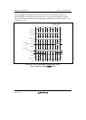
Burst read/single write (burst length 1) and burst read/burst write (burst length 1) are supported as
the SDRAM operating mode.
Commands for SDRAM can be specified by RAS, CAS, RD/WR, and specific address signals.
These commands supports:
NOP
Auto-refresh (REF)
Self-refresh (SELF)
All banks pre-charge (PALL)
Specified bank pre-charge (PRE)
Bank active (ACTV)
Read (READ)
Read with pre-charge (READA)
Write (WRIT)
Write with pre-charge (WRITA)
Write mode register (MRS, EMRS)
The byte to be accessed is specified by DQMU and DQML. Reading or writing is performed for a
byte whose corresponding DQMx is low. For details on the relationship between DQMx and the
byte to be accessed, see section 9.5.1, Endian/Access Size and Data Alignment.