


Section 27 Video Display Controller 3
R01UH0134EJ0400 Rev. 4.00 Page 1577 of 2108
Sep 24, 2014
SH7262 Group, SH7264 Group
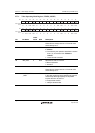
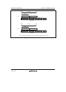
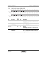
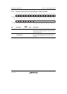
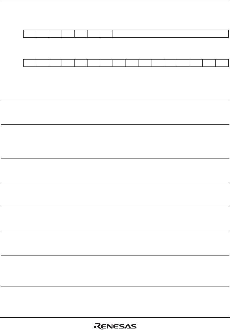
27.7.3 Video Input Timing Control Register (VIDEO_TIM_CNT)
31 30 29 28 27 26 25 24 23 22 21 20 19 18 17 16
15 14 13 12 11 10 9 8 7 6 5 4 3 2 1
0
0000000000000000
R R R R R R R R/W R/W R/W R/W R/W R/W R/W R/W R/W
0000000000000000
R R R R R R R R R R R/W R/W R R/W R/W R/W
------
-
- FIELD_SKEW[9:0]
----- ----
VSYNC_
TYP
HSYNC_
TYP
-
VSYNC_
TIM
HSYNC_
TIM
VIDEO_
TIM
Bit:
Initial value:
R/W:
Bit:
Initial value:
R/W:
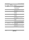
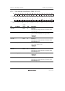
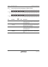
Bit Bit Name
Initial
Value R/W Description
31 to 26 All 0 R Reserved
These bits are always read as 0. The write value
should always be 0.
25 to 16 FIELD_SKEW
[9:0]
All 0 R/W These bits specify the timing of the VSYNC input
signal for the BT.601 input. When the VSYNC
signal is input within the DV_CLK cycles specified
in these bits before or after the HSYNC signal, it is
determined as the VSYNC signal for the TOP field.
15 to 6 All 0 R Reserved
These bits are always read as 0. The write value
should always be 0.
5 VSYNC_TYP 0 R/W Controls inversion of the DV_VSYNC input signal.
0: Not inverted
1: Input is inverted
4 HSYNC_TYP 0 R/W Controls inversion of the DV_HSYNC input signal.
0: Not inverted
1: Input is inverted
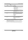
3 All 0 R Reserved
This bit is always read as 0. The write value should
always be 0.
2 VSYNC_TIM 0 R/W Specifies the timing of the DV_VSYNC input
signal.
0: Latched at the rising edge of the DV_CLK.
1: Latched at the falling edge of the DV_CLK.