


Page 2066 of 2108 R01UH0134EJ0400 Rev. 4.00
Sep 24, 2014
Item Page Revision (See Manual for Details)
5.3 Clock Operating Modes
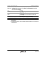
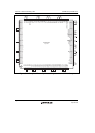
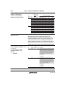
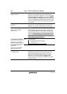
Table 5.3 Relationship
between Clock Operating
Mode and Frequency Range
121 Table amended
Clock
Operating
Mode
FRQCR
Setting*
1
PLL
Frequency
Multiplier
Ratio of
Internal
Clock
Frequencies
(I:B:P)*
2
Selectable Frequency Range (MHz)
PLL
Circuit
Input Clock*
3
Output Clock
(CKIO Pin)
CPU Clock
(Iφ)
Bus Clock
(Bφ)
Peripheral
Clock (Pφ)
2 H'x003 ON (× 8) 8:4:2 10 to 18 40 to 72 80 to 144 40 to 72 20 to 36
H'x004 ON (× 8) 8:4:4/3 10 to 18 40 to 72 80 to 144 40 to 72 13.33 to 24
H'x005 ON (× 8) 8:4:1 10 to 18 40 to 72 80 to 144 40 to 72 10 to 18
H'x006 ON (× 8) 8:4:2/3 10 to 18 40 to 72 80 to 144 40 to 72 6.67 to 12
H'x013 ON (× 8) 4:4:2 10 to 18 40 to 72 40 to 72 40 to 72 20 to 36
H'x014 ON (× 8) 4:4:4/3 10 to 18 40 to 72 40 to 72 40 to 72 13.33 to 24
H'x015 ON (× 8) 4:4:1 10 to 18 40 to 72 40 to 72 40 to 72 10 to 18
H'x016 ON (× 8) 4:4:2/3 10 to 18 40 to 72 40 to 72 40 to 72 6.67 to 12
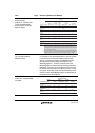
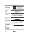
3 H'x003 ON (× 8) 8/3:4/3:2/3 48 64 128 64 32
H'x004 ON (× 8) 8/3:4/3:4/9 48 64 128 64 21.33
H'x005 ON (× 8) 8/3:4/3:1/3 48 64 128 64 16
H'x006 ON (× 8) 8/3:4/3:2/9 48 64 128 64 10.67
H'x013 ON (× 8) 4/3:4/3:2/3 48 64 64 64 32
H'x014 ON (× 8) 4/3:4/3:4/9 48 64 64 64 21.33
H'x015 ON (× 8) 4/3:4/3:1/3 48 64 64 64 16
H'x016 ON (× 8) 4/3:4/3:2/9 48 64 64 64 10.67
5.8.1 Note on Using a PLL
Oscillation Circuit
129 Description added
Since the analog power supply pins of the PLL are
sensitive to the noise, the system may malfunction due to
inductive interference at the other power supply pins. To
prevent such malfunction, the analog power supply pins
and the digital power supply pins Vcc and PVcc should not
supply the same resources on the board if at all possible.
Ensure that PLLVcc has the same electric potential as Vcc.
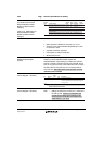
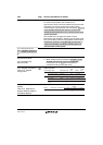
9.4.3 CSn Space Wait
Control Register (CSnWCR)
(n = 0 to 6)
(1) Normal Space, SRAM
with Byte Selection, and
MPX-I/O
CS5WCR
260,
261
Table amended
Bit Bit Name
Initial
Value
R/W Description
12, 11 SW[1:0] 00 R/W Number of Delay Cycles from Address, CS
5
Assertion
to RD, WE Assertion
These bits specify the number of delay cycles from
address and CS5 assertion to RD and WEn assertion
when area 5 is specified as normal space or SRAM
with byte selection. They specify the number of delay
cycles from address cycle (Ta3) to RD and WEn
assertion when area 5 is specified as MPX-I/O.
00: 0.5 cycles
01: 1.5 cycles
10: 2.5 cycles
11: 3.5 cycles
1, 0 HW[1:0] 00 R/W Delay Cycles from RD, WEn Negation to Address,
CS5 Negation
These bits specify the number of delay cycles from
RD and WEn negation to address and CS5 negation
when area 5 is specified as normal space or SRAM
with byte selection. They specify the number of delay
cycles from RD and WEn negation to CS5 negation
when area 5 is specified as MPX-I/O.
00: 0.5 cycles
01: 1.5 cycles
10: 2.5 cycles
11: 3.5 cycles