


Section 15 Serial Communication Interface with FIFO
R01UH0134EJ0400 Rev. 4.00 Page 765 of 2108
Sep 24, 2014
SH7262 Group, SH7264 Group
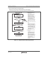
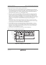
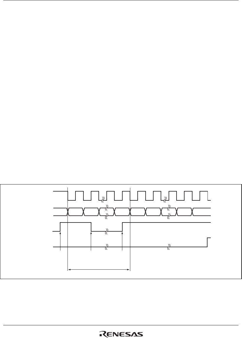
In serial transmission, this module operates as described below.
1. When data is written into the transmit FIFO data register (SCFTDR), the data is transferred
from SCFTDR to the transmit shift register (SCTSR). Confirm that the TDFE flag in the serial
status register (SCFSR) is set to 1 before writing transmit data to SCFTDR. The number of
data bytes that can be written is (16 – transmit trigger setting).
2. When data is transferred from SCFTDR to SCTSR and transmission is started, consecutive
transmit operations are performed until there is no transmit data left in SCFTDR. When the
number of transmit data bytes in SCFTDR falls below the transmit trigger number set in the
FIFO control register (SCFCR), the TDFE flag is set. If the TIE bit in the serial control register
(SCSR) is set to 1 at this time, a transmit-FIFO-data-empty interrupt (TXI) request is
generated.
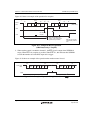
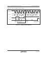
If clock output mode is selected, eight synchronous clock pulses are output. If an external
clock source is selected, data is output in synchronization with the input clock. Data is output
from the TxD pin in order from the LSB (bit 0) to the MSB (bit 7).
3. The SCFTDR transmit data is checked at the timing for sending the MSB (bit 7). If data is
present, the data is transferred from SCFTDR to SCTSR, and then serial transmission of the
next frame is started. If there is no data, the TxD pin holds the state after the TEND flag in
SCFSR is set to 1 and the MSB (bit 7) is sent.
4. After the end of serial transmission, the SCK pin is held in the high state.
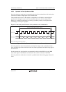
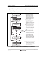
Figure 15.14 shows an example of transmit operation.
Serial clock
Serial data
TDFE
TEND
Data written to SCFTDR
and TDFE flag cleared
to 0 by TXI interrupt
handler
One frame
Bit 0
LSB
TXI
interrupt
request
MSB
Bit 1 Bit 6 Bit 7Bit 7 Bit 0 Bit 1
TXI
interrupt
request
Figure 15.14 Example of Transmit Operation