


Section 1 Overview
Page 14 of 2108 R01UH0134EJ0400 Rev. 4.00
Sep 24, 2014
SH7262 Group, SH7264 Group
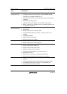
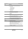
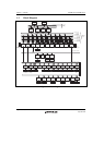
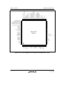
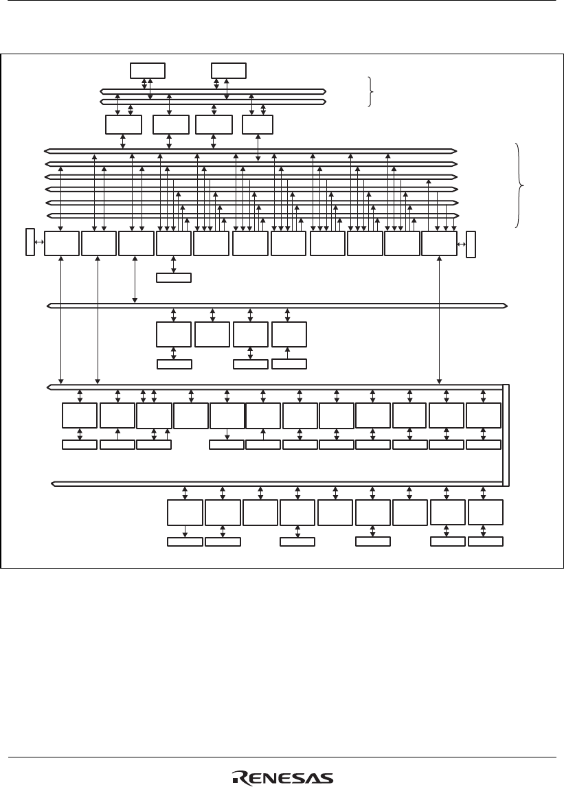
1.3 Block Diagram
SH-2A
CPU core
Floating-point
unit
Cache
controller
DMA
controller
Peripheral
bus 1
controller
Peripheral
bus 0
controller
Bus state
controller
Renesas
serial peripheral
interface
Large-capacity
on-chip RAM0
Large-capacity
on-chip RAM1
Large-capacity
on-chip RAM2
Large-capacity
on-chip RAM3
Large-capacity
on-chip RAM4
Large-capacity
on-chip RAM5
Video display
controller 3
Instruction
cache memory
8KB
Operand
cache memory
8KB
High-speed
on-chip RAM
64KB
Port
Port
Port
External bus input/output
Port
Serial I/O
Port
USB bus I/O
USB clock input
CPU memory access bus (M bus)
CPU instruction fetch bus (F bus)
CPU bus
(C bus)
(I clock)
Internal CPU bus
(IC-BUS)
Internal DMA bus
(ID-BUS)
Internal graphic bus 1
(IV1-BUS)
Internal graphic bus 2
(IV2-BUS)
Internal graphic bus 3
(IV3-BUS)
Internal graphic bus 4
(IV4-BUS)
Internal bus
(I bus)
(B clock)
DREQ input
DACK output
TEND output
Operation input
LCD I/F input/output
Peripheral bus 0 (B clock)
Peripheral bus 1 (P clock)
CD-ROM
decoder
USB 2.0
host/function
module
Port
Port Port Port Port Port Port
Port Port
EXTAL input
XTAL
output
CKIO I/O
Clock mode input
RES
input
NMI
input
IRQ
input
PINT
input
Timer pulse
I/O
Port
Port
RTC_X1 input
RTC_X
output
WDTOVF output
Port Port Port Port Port Port
Serial
I/O
CAN bus
I/O
IEBus I/O
audio clock
input
Serial I/O
audio clock
input
Serial I/O
audio clock
input
Serial I/O
audio clock input
I
2
C bus
I/O
Clock pulse
generator
Interrupt
controller
Compare
match
timer
Multi-funciton
timer pulse
unit 2
Watchdog
timer
Serial
sound
interface
Controller area
network
IEBus
TM
controller
Realtime
clock
Serial
communication
interface
with FIFL
Serial I/O
with FIFO
I
2
C bus
interface 3
User debugging
interface
Motor control
PWM timer
Power-down
mode control
General
I/O port
General I/O
Decompression
unit
Sampling
rate converter
SD host
interface
NAND
flash memory
controller
Renesas
SPDIF
interface
JTAG I/O
Timer pulse
output
SD card interface
I/O
Flash memory
interface I/O
Port
A/D converter
Analog input
ADTRG input
Figure 1.1 Block Diagram