Section 10 Direct Memory Access Controller
Page 384 of 2108 R01UH0134EJ0400 Rev. 4.00
Sep 24, 2014
SH7262 Group, SH7264 Group
10.3.1 DMA Source Address Registers (SAR)
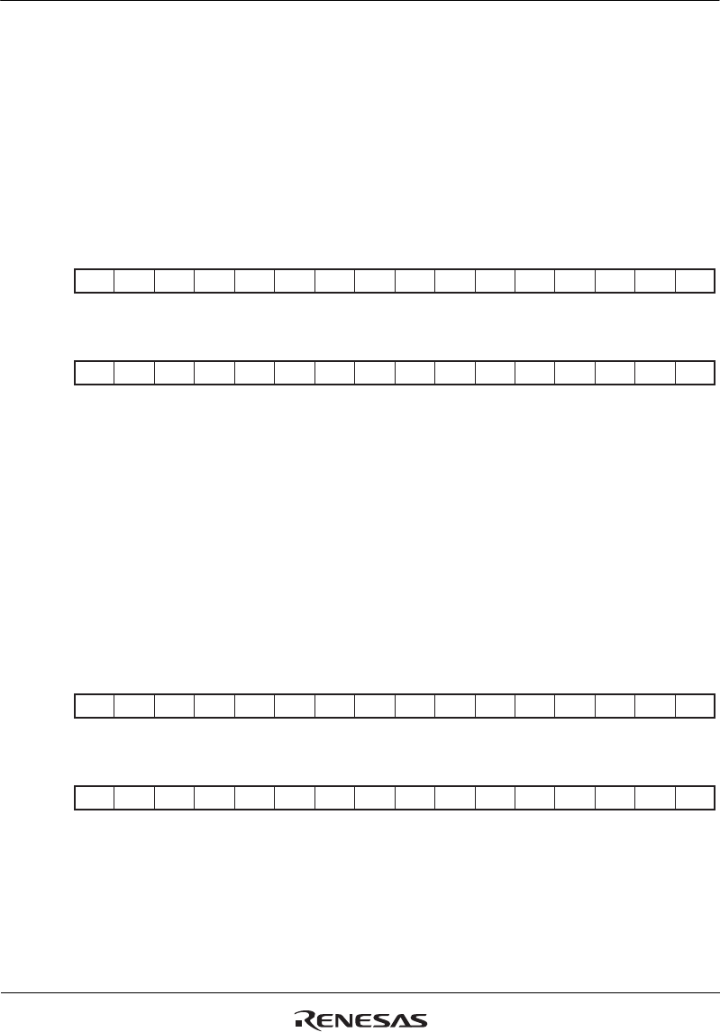
The DMA source address registers (SAR) are 32-bit readable/writable registers that specify the
source address of a DMA transfer. During a DMA transfer, these registers indicate the next source
address. When the data of an external device with DACK is transferred in single address mode,
SAR is ignored.
To transfer data in word (2-byte), longword (4-byte), or 16-byte unit, specify the address with 2-
byte, 4-byte, or16-byte address boundary respectively.
31 30 29 28 27 26 25 24 23 22 21 20 19 18 17 16
15 14 13 12 11 10 9 8 7 6 5 4 3 2 1
0
0000000000000000
R/W R/W R/W R/W R/W R/W R/W R/W R/W R/W R/W R/W R/W R/W R/W R/W
0000000000000000
R/W R/W R/W R/W R/W R/W R/W R/W R/W R/W R/W R/W R/W R/W R/W R/W
Bit:
Initial value:
R/W:
Bit:
Initial value:
R/W:
----------------
----------------
10.3.2 DMA Destination Address Registers (DAR)
The DMA destination address registers (DAR) are 32-bit readable/writable registers that specify
the destination address of a DMA transfer. During a DMA transfer, these registers indicate the
next destination address. When the data of an external device with DACK is transferred in single
address mode, DAR is ignored.
To transfer data in word (2-byte), longword (4-byte), or 16-byte unit, specify the address with 2-
byte, 4-byte, or 16-byte address boundary respectively.
31 30 29 28 27 26 25 24 23 22 21 20 19 18 17 16
15 14 13 12 11 10 9 8 7 6 5 4 3 2 1
0
0000000000000000
R/W R/W R/W R/W R/W R/W R/W R/W R/W R/W R/W R/W R/W R/W R/W R/W
0000000000000000
R/W R/W R/W R/W R/W R/W R/W R/W R/W R/W R/W R/W R/W R/W R/W R/W
Bit:
Initial value:
R/W:
Bit:
Initial value:
R/W:
----------------
----------------


