


Section 32 General Purpose I/O Ports
R01UH0134EJ0400 Rev. 4.00 Page 1747 of 2108
Sep 24, 2014
SH7262 Group, SH7264 Group
32.2.25 Port G I/O Registers 0, 1 (PGIOR0, PGIOR1)
PGIOR1 and PGIOR0 are 16-bit readable/writable registers that are used to set the pins on port G
as inputs or outputs. The PG24IOR to PG0IOR bits correspond to the PG24 to PG0, respectively.
PGIOR1 and PGIOR0 are enabled when the port G pins are functioning as general-purpose I/O
(PG24 to PG0) or TIOC I/O of multi-function timer pulse unit 2. In other states, they are disabled.
If bits in PGIOR1 and PGIOR0 are set to 1, corresponding pins on port G functions as outputs. If
they are cleared to 0, the corresponding pins function as inputs.
Bits15 to 9 in PGIOR1, and bits 8 to 5 in PGIOR1 in the SH7262 Group are reserved. These bits
are always read as 0. The write values should always be 0.
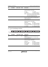
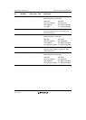
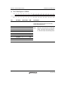
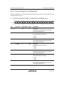
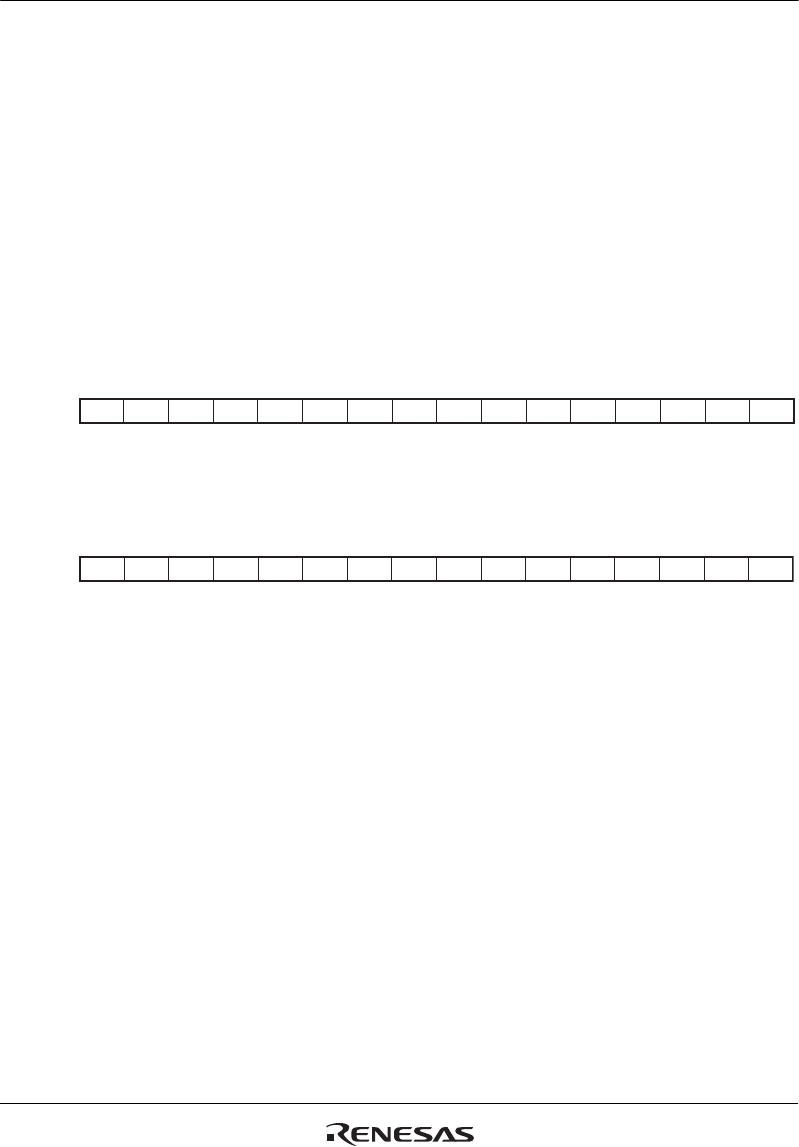
(1) Port G IO Register 1 (PGIOR1)
15 14 13 12 11 10 9 8 7 6 5 4 3 2 1 0
0000000000000000
RRRRRRRR/WR/WR/WR/WR/WR/WR/WR/WR/W
------
PG24
IOR
PG23
IOR
PG22
IOR
PG21
IOR
PG20
IOR
PG19
IOR
PG18
IOR
PG17
IOR
PG16
IOR
-
Bit:
Initial value:
R/W:
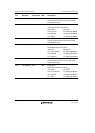
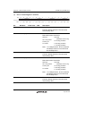
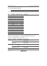
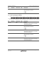
(2) Port G IO Register 0 (PGIOR0)
15 14 13 12 11 10 9 8 7 6 5 4 3 2 1 0
0000000000000000
R/W R/W R/W R/W R/W R/W R/W R/W R/W R/W R/W R/W R/W R/W R/W R/W
PG15
IOR
PG14
IOR
PG13
IOR
PG12
IOR
PG11
IOR
PG10
IOR
PG9
IOR
PG8
IOR
PG7
IOR
PG6
IOR
PG5
IOR
PG4
IOR
PG3
IOR
PG2
IOR
PG1
IOR
PG0
IOR
Bit:
Initial value:
R/W:
32.2.26 Port G Data Register 0, 1 (PGDR0, PGDR1)
PGDR1 and PGDR0 are 16-bit readable/writable registers that store port G data. The PG24DR to
PG0DR bits correspond to the PG24 to PGDR0 pins, respectively.
When a pin function is general output, if a value is written to PGDR1 or PGDR0, that value is
output from the pin, and if PGDR1 or PGDR0 is read, the register value is returned directly
regardless of the pin state.
When a pin function is general input, if PGDR1 or PGDR0 is read, the pin state, not the register
value, is returned directly. If a value is written to PGDR1 or PGDR0, although that value is
written into PGDR1 or PGDR0, it does not affect the pin state. Table 32.19 summarizes
PGDR1/PGDR0 read/write operation.