Section 5 Clock Pulse Generator
R01UH0134EJ0400 Rev. 4.00 Page 129 of 2108
Sep 24, 2014
SH7262 Group, SH7264 Group
5.8 Notes on Board Design
5.8.1 Note on Using a PLL Oscillation Circuit
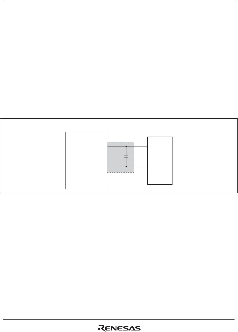
In the PLLVcc and PLLVss connection pattern for the PLL, signal lines from the board power
supply pins must be as short as possible and pattern width must be as wide as possible to reduce
inductive interferences.
Since the analog power supply pins of the PLL are sensitive to the noise, the system may
malfunction due to inductive interference at the other power supply pins. To prevent such
malfunction, the analog power supply pins and the digital power supply pins Vcc and PVcc should
not supply the same resources on the board if at all possible.
Ensure that PLLVcc has the same electric potential as Vcc.
PLLVcc
PLLVss
Vcc
Vss
Power supply
Signal lines prohibited
Figure 5.4 Note on Using a PLL Oscillation Circuit


