


Section 31 On-Chip RAM
R01UH0134EJ0400 Rev. 4.00 Page 1671 of 2108
Sep 24, 2014
SH7262 Group, SH7264 Group
Section 31 On-Chip RAM
This LSI has an on-chip high-speed RAM, which achieves fast access, an on-chip large-capacity
RAM for display area and work area (32 Kbytes for 1-Mbyte version and 320 Kbytes for 640-
Kbyte version of this RAM are shared with the on-chip data retention RAM), and an on-chip data
retention RAM, which can retain data in deep standby mode. These memory units can be used to
store instructions or data.
The operation and write access to the on-chip high-speed RAM and large-capacity RAM
(including on-chip data retention RAM) can be enabled or disabled through the RAM enable bits
and RAM write enable bits.
The on-chip data retention RAM is assigned to page 5 for 1-Mbyte and page 0 to 2 for 640-Kbyte
versions of the on-chip large-capacity RAM. Retention or non-retention of data by the on-chip
data retention RAM in deep standby mode is selectable on a per-page basis.
31.1 Features
Page
The on-chip high-speed RAM consists of four pages. The size of one page is 16 Kbytes.
The size of each page is determined depending on the display area sizes (QVGA,
WQVGA, and VGA sizes).
The on-chip data retention RAM consists of two pages for 1-Mbyte and four pages for 640-
Kbyte versions. For 1-Mbyte version, the size of each page is 16-Kbytes. For 640-Kbyte
version, page 0 has 16-Kbytes, page 1 has 16-Kbytes, page 2 has 128-Kbytes, and page 3
has 160-Kbytes.
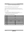
Memory map
The on-chip RAM is located in the address spaces shown in tables 31.1 to 31.5.
Table 31.1 Address Spaces of On-Chip High-Speed RAM
Page Address
Page 0 H'FFF80000 to H'FFF83FFF
Page 1 H'FFF84000 to H'FFF87FFF
Page 2 H'FFF88000 to H'FFF8BFFF
Page 3 H'FFF8C000 to H'FFF8FFFF