


Section 33 Power-Down Modes
R01UH0134EJ0400 Rev. 4.00 Page 1793 of 2108
Sep 24, 2014
SH7262 Group, SH7264 Group
33.2.13 System Control Register 4 (SYSCR4)
SYSCR4 is an 8-bit readable/writable register that enables or disables writing to a specified page
in the large-capacity on-chip RAM.
When a VRAMWEn (n = 0 to 5) bit is set to 1, writing to page n is enabled. When a VRAMWEn
bit is cleared to 0, writing to page n is ignored. The initial value of a VRAMWEn bit is 1.
SYSCR4 should be set with a program located in an area other than the large-capacity on-chip RAM. Furthermore, an
instruction to read SYSCR4 should be located immediately after the instruction to write to SYSCR4. If not, normal access
is not guaranteed.
Note: When writing to this register, see section 33.4, Usage Notes.
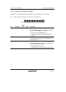
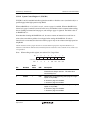
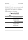
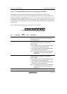
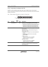
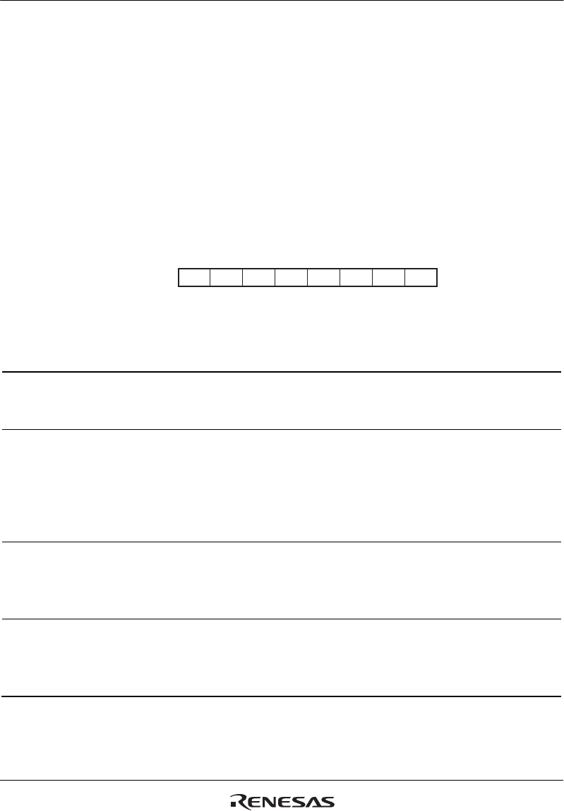
76543210
Bit:
Initial value:
R/W:
11111111
R R R/W R/W R/W R/W R/W R/W
--
VRAM
WE5
VRAM
WE4
VRAM
WE3
VRAM
WE2
VRAM
WE0
VRAM
WE1
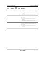
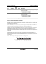
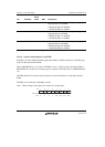
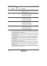
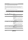
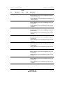
Bit Bit Name
Initial
Value
R/W Description
7, 6 All 1 R Reserved
These bits are always read as 1. The write value
should always be 1.
5 VRAMWE5 1 R/W RAM Write Enable 5 (corresponding area: page 5* in
large-capacity on-chip RAM)
0: Writing to page 5 is disabled.
1: Writing to page 5 is enabled.
Note: This bit is reserved in 640-Kbyte version and
read as 1. The write value should always be 0.
4 VRAMWE4 1 R/W RAM Write Enable 4 (corresponding area: page 4* in
large-capacity on-chip RAM)
0: Writing to page 4 is disabled.
1: Writing to page 4 is enabled.
3 VRAMWE3 1 R/W RAM Write Enable 3 (corresponding area: page 3* in
large-capacity on-chip RAM)
0: Writing to page 3 is disabled.
1: Writing to page 3 is enabled.