


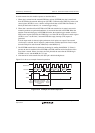

Section 15 Serial Communication Interface with FIFO
R01UH0134EJ0400 Rev. 4.00 Page 763 of 2108
Sep 24, 2014
SH7262 Group, SH7264 Group
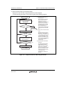
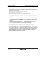
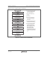
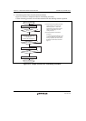
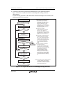
Figure 15.12 shows a sample flowchart for initialization.
Start of initialization
Clear TE and RE bits
in SCSCR to 0
Set TFRST and RFRST bits
in SCFCR to 1 to clear
the FIFO buffer
After reading ER, DR,
and BRK flags in SCFSR,
write 0 to clear them
Set CKE[1:0] in SCSCR
(leaving TIE, RIE, TE,
and RE bits cleared to 0)
Set data transfer format
in SCSMR
Set the general I/O port external pins used
SCK, TxD, RxD
Set value in SCBRR
Set RTRG[1:0] and TTRG[1:0] bits
in SCFCR, and clear TFRST
and RFRST bits to 0
Set TE and RE bits in SCSCR
to 1, and set TIE, RIE,
and REIE bits
End of initialization
Leave the TE and RE bits cleared
to 0 until the initialization almost
ends. Be sure to clear the TIE,
RIE, TE, and RE bits to 0.
Set the data transfer format in
SCSMR.
Set CKE[1:0].
Write a value corresponding to
the bit rate into SCBRR. This
is not necessary if an external
clock is used.
Sets the general I/O port external
pins used. Set as RxD input at
receiving and TxD at transmission.
Set the TE or RE bit in SCSCR
to 1. Also set the TIE, RIE, and
REIE bits to enable the TxD,
RxD, and SCK pins to be used.
When transmitting, the TxD pin
will go to the mark state.
When receiving in clocked
synchronous mode with the
synchronization clock output (clock
master) selected, a clock starts to
be output from the SCK pin at this
point.
[1]
[1]
[2]
[3]
[4]
[5]
[6]
[2]
[3]
[4]
[5]
[6]
Figure 15.12 Sample Flowchart for Initialization