


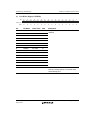
Section 32 General Purpose I/O Ports
R01UH0134EJ0400 Rev. 4.00 Page 1701 of 2108
Sep 24, 2014
SH7262 Group, SH7264 Group
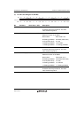
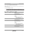
Bit Bit Name Initial Value R/W Description
7 to 5 All 0 R Reserved
These bits are always read as 0. The write
value should always be 0.
4 PB1MD0 0/1 R/W PB1 Mode
Select the function of the PB1.
Boot mode 0
0: Setting prohibited
1: A1 (initial value)
Boot mode 1 to 3
0: PB1 (initial value)
1: A1
3 to 0 All 0 R Reserved
These bits are always read as 0. The write
value should always be 0.
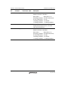
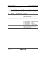
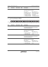
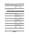
32.2.5 Port B I/O Registers 0, 1 (PBIOR0, PBIOR1)
PBIOR0 and PBIOR1 are 16-bit readable/writable registers that are used to set the pins on port B
as inputs or outputs. The PB22IOR to PB1IOR bits correspond to the PB22 to PB1 pins,
respectively. PBIOR1 and PBIOR0 are enabled when the port B pins are functioning as general-
purpose I/O (PB22 to PB1) or TIOC I/O of multi-function timer pulse unit 2. In other states, they
are disabled. If a bit in PBIOR1 or PBIOR0 is set to 1, the corresponding pin on port B functions
as output pin. If it is cleared to 0, the corresponding pin functions as an input pin.
Bits 15 to 7 in PBIOR1 and bit 0 in PBIOR0 are reserved. These bits are always read as 0. The
write value should always be 0.
(1) Port B I/O Register 1 (PBIOR1)
1514131211109876543210
0000000000000000
RRRRRRRRRR/WR/WR/WR/WR/WR/WR/W
--------
PB22
IOR
PB21
IOR
PB20
IOR
PB19
IOR
PB18
IOR
PB17
IOR
PB16
IOR
-
Bit:
Initial value:
R/W:
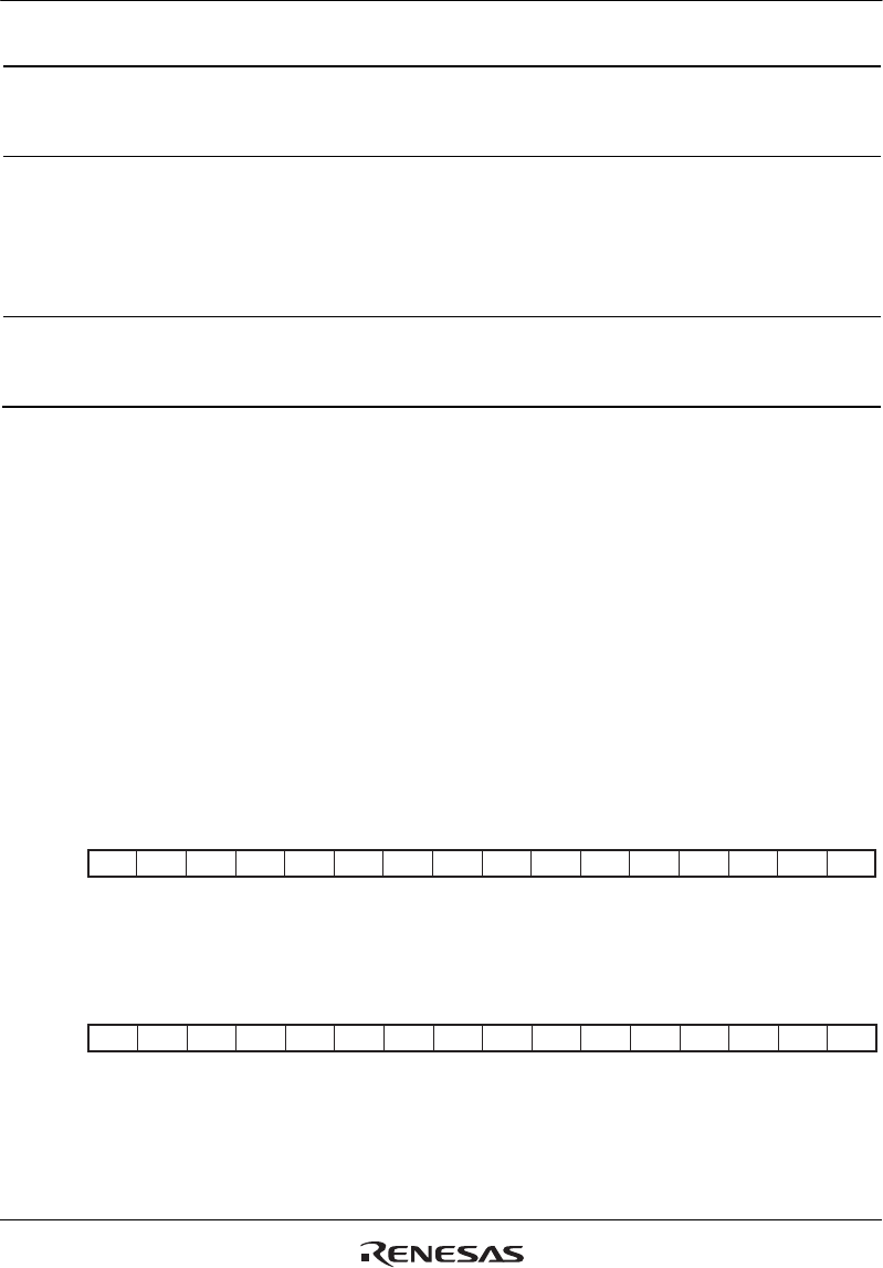
(2) Port B I/O Register 0 (PBIOR0)
15 14 13 12 11 10 9 8 7 6 5 4 3 2 1 0
0000000000000000
R/W R/W R/W R/W R/W R/W R/W R/W R/W R/W R/W R/W R/W R/W R/W R
PB15
IOR
PB14
IOR
PB13
IOR
PB12
IOR
PB11
IOR
PB10
IOR
PB9
IOR
PB8
IOR
PB7
IOR
PB6
IOR
PB5
IOR
PB4
IOR
PB3
IOR
PB2
IOR
PB1
IOR
-
Bit:
Initial value:
R/W: