


Section 10 Direct Memory Access Controller
Page 430 of 2108 R01UH0134EJ0400 Rev. 4.00
Sep 24, 2014
SH7262 Group, SH7264 Group
10.5 Usage Notes
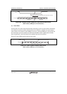
10.5.1 Timing of DACK and TEND Outputs
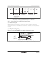
When the external memory is the MPX-I/O, the DACK output is asserted with the timing of the
data cycle. For details, see section 9.5.5, MPX-I/O Interface in section 9, Bus State Controller.
When the memory is other than the MPX-I/O, the DACK output is asserted with the same timing
as the corresponding CS signal.
The TEND output does not depend on the type of memory and is always asserted with the same
timing as the corresponding CS signal.
10.5.2 Notes on Using Flag Bits
The notes on using the following flag bits are described here.
DMA channel control register (CHCR)
HE (Half-End) and TE (Transfer End Flag) bits
DMA operation register (DMAOR)
AE (Address Error Flag) and NMIF (NMI Flag) bits
If a flag is read at the same timing it is set to 1, the read data will be 0, but the internal state may
be the same as reading 1. Therefore, if 0 is written to the flag, the flag will be cleared to 0 because
the internal state is the same as when writing 0 after reading 1.
In the case of using a flag, to prevent from unintentionally clearing the flag bit to 0, perform
read/write as follows:
(a) In the case of intended bit clear, write 0 to the flag bit after reading it as 1.
(b) In other cases, write 1 to the flag bit.
If a flag is not used, just writing 0 to the flag bit does not generate errors (in the case of intended
bit clear, write 0 to the flag bit after reading it as 1).