


Section 11 Multi-Function Timer Pulse Unit 2
Page 544 of 2108 R01UH0134EJ0400 Rev. 4.00
Sep 24, 2014
SH7262 Group, SH7264 Group
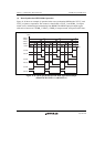
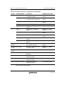
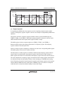
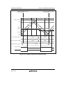
Counter value
TGRA_3
TCDR
TDDR
H'0000
TCNT_4
TCNTS
TCNT_3
TCNT_3
TCNT_4
TCNTS
Time
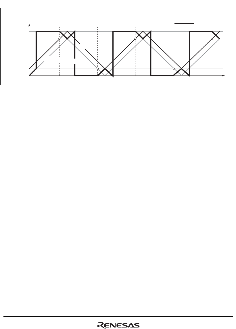
Figure 11.39 Complementary PWM Mode Counter Operation
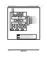
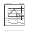
(b) Register Operation
In complementary PWM mode, nine registers are used, comprising compare registers, buffer
registers, and temporary registers. Figure 11.40 shows an example of complementary PWM mode
operation.
The registers which are constantly compared with the counters to perform PWM output are
TGRB_3, TGRA_4, and TGRB_4. When these registers match the counter, the value set in bits
OLSN and OLSP in the timer output control register (TOCR) is output.
The buffer registers for these compare registers are TGRD_3, TGRC_4, and TGRD_4.
Between a buffer register and compare register there is a temporary register. The temporary
registers cannot be accessed by the CPU.
Data in a compare register is changed by writing the new data to the corresponding buffer register.
The buffer registers can be read or written at any time.
The data written to a buffer register is constantly transferred to the temporary register in the Ta
interval. Data is not transferred to the temporary register in the Tb interval. Data written to a
buffer register in this interval is transferred to the temporary register at the end of the Tb interval.
The value transferred to a temporary register is transferred to the compare register when TCNTS
for which the Tb interval ends matches TGRA_3 when counting up, or H'0000 when counting
down. The timing for transfer from the temporary register to the compare register can be selected
with bits MD3 to MD0 in the timer mode register (TMDR). Figure 11.40 shows an example in
which the mode is selected in which the change is made in the trough.