


Section 9 Bus State Controller
R01UH0134EJ0400 Rev. 4.00 Page 355 of 2108
Sep 24, 2014
SH7262 Group, SH7264 Group
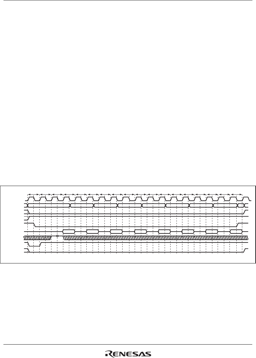
9.5.10 Burst ROM (Clocked Synchronous) Interface
The burst ROM (clocked synchronous) interface is supported to access a ROM with a
synchronous burst function at high speed. The burst ROM interface accesses the burst ROM in the
same way as a normal space. This interface is valid only for area 0.
In the first access cycle, wait cycles are inserted. In this case, the number of wait cycles to be
inserted is specified by the W3 to W0 bits in CS0WCR. In the second and subsequent cycles, the
number of wait cycles to be inserted is specified by the BW1 and BW0 bits in CS0WCR.
While the burst ROM (clocked synchronous) is accessed, the BS signal is asserted only for the
first access cycle and an external wait input is also valid for the first access cycle.
Since the bus width is 16 bits, the burst length must be specified as 8. The burst ROM interface
does not support the 8-bit bus width for the burst ROM.
The burst ROM interface performs burst operations for all read access. For example, in a
longword access over a 16-bit bus, valid 16-bit data is read two times and invalid 16-bit data is
read six times. These invalid data read cycles increase the memory access time and degrade the
program execution speed and DMA transfer speed. To prevent this problem, it is recommended
using a 16-byte read by cache fill in the cache-enabled spaces or 16-byte read by the DMA. The
burst ROM interface performs write access in the same way as normal space access.
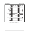
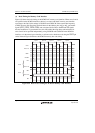
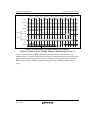
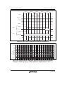
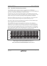
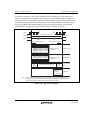
TwbT1 T2Tw T2BTw T2B Twb TwbT2B T2B Twb TwbT2B T2B Twb T2B Twb
Note: * The waveform for DACKn is when active low is specified.
CKIO
CS0
RD/WR
A25 to A0
RD
D15 to D0
WAIT
BS
DACKn*
Figure 9.44 Burst ROM Access Timing (Clocked Synchronous)
(Burst Length = 8, Wait Cycles Inserted in First Access = 2,
Wait Cycles Inserted in Second and Subsequent Access Cycles = 1)