


Section 11 Multi-Function Timer Pulse Unit 2
R01UH0134EJ0400 Rev. 4.00 Page 613 of 2108
Sep 24, 2014
SH7262 Group, SH7264 Group
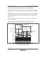
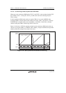
11.7.20 Output Level in Complementary PWM Mode and Reset-Synchronized PWM Mode
When channels 3 and 4 are in complementary PWM mode or reset-synchronized PWM mode, the
PWM waveform output level is set with the OLSP and OLSN bits in the timer output control
register (TOCR). In the case of complementary PWM mode or reset-synchronized PWM mode,
TIOR should be set to H'00.
11.7.21 Interrupts in Module Standby Mode
If module standby mode is entered when an interrupt has been requested, it will not be possible to
clear the CPU interrupt source or the direct memory access controller activation source. Interrupts
should therefore be disabled before entering module standby mode.
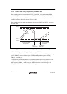
11.7.22 Simultaneous Capture of TCNT_1 and TCNT_2 in Cascade Connection
When timer counters 1 and 2 (TCNT_1 and TCNT_2) are operated as a 32-bit counter in cascade
connection, the cascade counter value cannot be captured successfully even if input-capture input
is simultaneously done to TIOC1A and TIOC2A or to TIOC1B and TIOC2B. This is because the
input timing of TIOC1A and TIOC2A or of TIOC1B and TIOC2B may not be the same when
external input-capture signals to be input into TCNT_1 and TCNT_2 are taken in synchronization
with the internal clock. For example, TCNT_1 (the counter for upper 16 bits) does not capture the
count-up value by overflow from TCNT_2 (the counter for lower 16 bits) but captures the count
value before the count-up. In this case, the values of TCNT_1 = H'FFF1 and TCNT_2 = H'0000
should be transferred to TGRA_1 and TGRA_2 or to TGRB_1 and TGRB_2, but the values of
TCNT_1 = H'FFF0 and TCNT_2 = H'0000 are erroneously transferred.